TI-DS99R421-Q1.pdf

需积分: 0 7 浏览量
更新于2023-02-07
4
收藏 918KB PDF 举报
FPD-Link转换器DS99R421-Q1
FPD-Link转换器DS99R421-Q1是一款由德州仪器(TI)公司推出的高速串行转换器,旨在将FPD-Link信号转换为FPD-Link II信号。该器件具有多种特性,能够满足不同应用场景的需求。
功能描述:
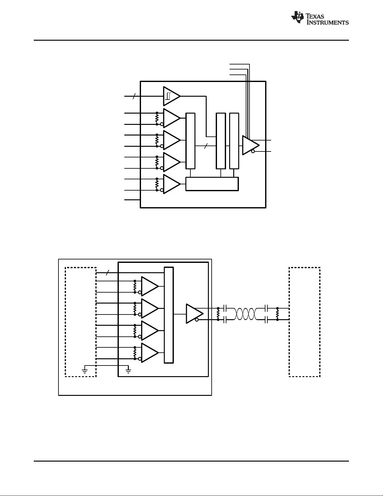
DS99R421-Q1的主要功能是将FPD-Link信号转换为FPD-Link II信号,实现高速数据传输。该器件可以将3个LVDS数据信号和1个LVDS时钟信号转换为单个LVDS串行流,嵌入时钟信息。该串行流可以通过单个差分对PCB迹线和电缆传输,解决了LVDS数据输入和LVDS时钟路径之间的时延问题。
特性:
FPD-Link转换器DS99R421-Q1具有以下特性:
* 用户可调整的预加重驱动能力,通过外部电阻在LVDS输出端实现
* 能够驱动长达10米的屏蔽双绞线电缆
* 支持AC耦合数据传输
* 集成了100Ω的LVDS终端电阻
* 电源关闭控制
* 可以与DS90UR124进行BIST测试以验证链路完整性
* 所有LVCMOS输入和控制引脚具有内部下拉电阻
* Schmitt触发器输入OS[2:0]以最小化不稳定条件
* 输出tri-state通过DEN输出使能
* PLL滤波器集成在芯片内
* 电源电压范围为3.3V ± 10%
* 工作温度范围为-40°C到+105°C
* 高达8kV的ESD耐受性
* 符合ISO 10605 ESD和AEC-Q100标准
应用场景:
FPD-Link转换器DS99R421-Q1广泛应用于各类高速数据传输系统,例如高分辨率显示器、机器视觉系统、医疗成像设备等。在这些应用场景中,FPD-Link转换器DS99R421-Q1能够提供高速、可靠的数据传输解决方案。
FPD-Link转换器DS99R421-Q1是一款功能强大、性能出色的高速串行转换器,能够满足不同应用场景的需求,广泛应用于高速数据传输系统。
DS99R421
www.ti.com
SNLS264D –JUNE 2007–REVISED APRIL 2013
5-43 MHz FPD-Link LVDS (3 Data + 1 Clock) to FPD-Link II LVDS (Embedded Clock DC-
Balanced) Converter
Check for Samples: DS99R421
1
FEATURES
DESCRIPTION
The DS99R421 converts a FPD-Link input with 4
2
• 5 MHz–43 MHz Embedded Clock & DC-
non-DC Balanced LVDS (3 LVDS Data + LVDS
Balanced Data Transmission (21 Total LVDS
Clock) plus 3 over-sampled low speed control bits
Data Bits Plus 3 Low Speed LVCMOS Data
into a single LVDS DC-balanced serial stream with
Bits)
embedded clock information. This single serial stream
• User Adjustable Pre-Emphasis Driving Ability
simplifies transferring the 24-bit bus over a single
Through External Resistor on LVDS Outputs
differential pair of PCB traces and cable by
eliminating the skew problems between the 3 parallel
and Capable to Drive up to 10 Meters Shielded
LVDS data inputs and LVDS clock paths. It saves
Twisted-Pair Cable
system cost by narrowing 4 LVDS pairs to 1 LVDS
• Supports AC-Coupling Data Transmission
pair that in turn reduce PCB layers, cable width,
• 100Ω Integrated Termination Resistor at LVDS
connector size, and pins.
Input
The DS99R421 incorporates a single serialized LVDS
• Power-Down Control
signal on the high-speed I/O. Embedded clock LVDS
• Available @SPEED BIST to DS90UR124 to
provides a low power and low noise environment for
Validate Link Integrity
reliably transferring data over a serial transmission
path. By optimizing the converter output edge rate for
• All LVCMOS Inputs & Control Pins Have
the operating frequency range EMI is further reduced.
Internal Pulldown
In addition the device features pre-emphasis to boost
• Schmitt Trigger Inputs on OS[2:0] to Minimize
signals over longer distances using lossy cables.
Metastable Conditions
Internal DC balanced encoding is used to support
• Outputs Tri-Stated Through DEN
AC-Coupled interconnects.
• On-Chip Filters for PLLs
• Power Supply Range 3.3V ± 10%
• Automotive Temperature Range −40°C to
+105°C
• Greater Than 8kV ESD Tolerance
• Meets ISO 10605 ESD and AEC-Q100
Compliance
1
Please be aware that an important notice concerning availability, standard warranty, and use in critical applications of
Texas Instruments semiconductor products and disclaimers thereto appears at the end of this data sheet.
2All trademarks are the property of their respective owners.
PRODUCTION DATA information is current as of publication date.
Copyright © 2007–2013, Texas Instruments Incorporated
Products conform to specifications per the terms of the Texas
Instruments standard warranty. Production processing does not
necessarily include testing of all parameters.

剩余25页未读,继续阅读
166 浏览量
107 浏览量
134 浏览量
2023-02-07 上传
2023-02-01 上传
118 浏览量
2023-02-01 上传
2023-02-01 上传
2023-02-01 上传
147 浏览量
177 浏览量
2023-02-01 上传
资源评论


不觉明了
- 粉丝: 6600
- 资源: 5764


最新资源
- 4b126基于Springboot+vue的新闻发布管理系统_springboot+vue.zip
- 4b128高校院系学生信息管理系统设计与实现_springboot+vue.zip
- 4b125智慧旅游系统_springboot+vue.zip
- 4b132基于软件研发过程中的缺陷管理系统的设计与实现_springboot+vue.zip
- 4b131小区车辆管理系统-springboot+vue.zip
- 4b129基于springboot+vue的宠物寄养系统.zip
- 4b134校园车辆管理系统_springboot+vue.zip
- Windows 7 离线补丁包 - UpdatePack7R2(24.12.12)珍藏品
- CRT8.7中文版,解压直接使用,不用安装
- 智能合约技术:基于Solidity的数据存储与访问权限管理
- COMSOL电线缆,电磁涡流感应热仿真,集肤效应,涡流效应仿真
- 4b041考试报名系统_springboot+vue0.zip
- 2-SvgToXaml-WPF开发者实用工具
- 4b055在线考试系统_springboot+vue0.zip
- 4b050明星周边商城系统_springboot+vue0.zip
- 4b070水果蔬菜商城_springboot+vue0.zip
