没有合适的资源?快使用搜索试试~ 我知道了~
TI-SN74CBTLV1G125-Q1.pdf
需积分: 5 0 下载量 59 浏览量
2022-12-02
00:00:03
上传
评论 4
收藏 1.19MB PDF 举报
温馨提示
试读
17页
TI-SN74CBTLV1G125-Q1.pdf
资源推荐
资源详情
资源评论
C
or
System Logic
B
GND
2.5 V
A
V
CC
C
To/From
System
Product
Folder
Order
Now
Technical
Documents
Tools &
Software
Support &
Community
本文档旨在为方便起见,提供有关 TI 产品中文版本的信息,以确认产品的概要。 有关适用的官方英文版本的最新信息,请访问 www.ti.com,其内容始终优先。 TI 不保证翻译的准确
性和有效性。 在实际设计之前,请务必参考最新版本的英文版本。
English Data Sheet: SCDS289
SN74CBTLV1G125-Q1
ZHCSJ80B –AUGUST 2009–REVISED JANUARY 2019
SN74CBTLV1G125-Q1 低低电电压压单单路路 FET 总总线线开开关关
1
1 特特性性
1
• 符合面向汽车应用的 应用
– 器件温度等级 1:
–40°C 至 +125°C,T
A
• 两个端口间使用 5Ω 开关连接
• 支持在数据 I/O 端口进行轨至轨开关
• I
off
支持局部断电模式运行
2 应应用用
• 呼吸机
3 说说明明
SN74CBTLV1G125 采用 单路高速线路开关。当输出
使能 (OE) 输入为高电平时,开关被禁用。
该器件完全 适用于 使用 I
off
的局部断电应用。I
off
特性
确保在关断时防止损坏电流通过器件回流。该器件可在
关断时提供隔离。
为了确保加电或断电期间的高阻抗状态,OE 应通过一
个上拉电阻器被连接至 V
CC
;该电阻器的最小值由驱动
器的电流吸入能力来决定。
器器件件信信息息
(1)
订订货货编编号号 封封装装 封封装装尺尺寸寸
SN74CBTLV1G125-Q1 SOT-23 (DBV) (5)
2.90mm ×
1.60mm
(1) 如需了解所有可用封装,请参阅数据表末尾的可订购产品附
录。
应应用用原原理理图图
2
SN74CBTLV1G125-Q1
ZHCSJ80B –AUGUST 2009 –REVISED JANUARY 2019
www.ti.com.cn
Copyright © 2009–2019, Texas Instruments Incorporated
目目录录
1 特特性性.......................................................................... 1
2 应应用用.......................................................................... 1
3 说说明明.......................................................................... 1
4 修修订订历历史史记记录录 ........................................................... 2
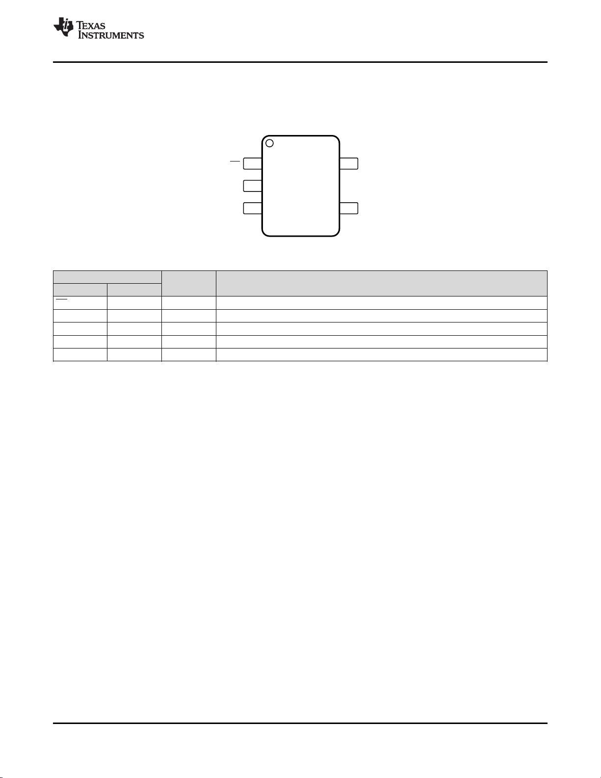
5 Pin Configuration and Functions......................... 3
6 Specifications......................................................... 4
6.1 Absolute Maximum Ratings ..................................... 4
6.2 ESD Ratings.............................................................. 4
6.3 Recommended Operating Conditions ...................... 4
6.4 Thermal Information.................................................. 4
6.5 Electrical Characteristics........................................... 5
6.6 Switching Characteristics.......................................... 5
7 Parameter Measurement Information .................. 6
8 Detailed Description.............................................. 7
8.1 Overview ................................................................... 7
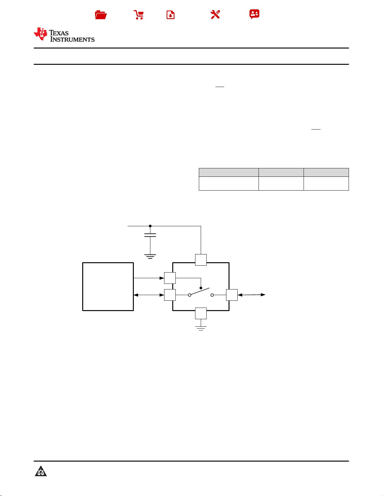
8.2 Functional Block Diagram ......................................... 7
8.3 Feature Description................................................... 7
8.4 Device Functional Modes.......................................... 7
9 Application and Implementation .......................... 8
9.1 Application Information.............................................. 8
9.2 Typical Application ................................................... 8
10 Power Supply Recommendations ....................... 9
11 Layout..................................................................... 9
11.1 Layout Guidelines ................................................... 9
11.2 Layout Example ...................................................... 9
12 器器件件和和文文档档支支持持 ..................................................... 10
12.1 器件支持 ............................................................... 10
12.2 接收文档更新通知 ................................................. 10
12.3 社区资源................................................................ 10
12.4 商标 ....................................................................... 10
12.5 静电放电警告......................................................... 10
12.6 术语表 ................................................................... 10
13 机机械械、、封封装装和和可可订订购购信信息息....................................... 10
4 修修订订历历史史记记录录
注:之前版本的页码可能与当前版本有所不同。
Changes from Revision A (December 2018) to Revision B Page
• 将
特性
从“符合汽车类 应用” 更改为“符合面向汽车 应用的 AEC-Q100”................................................................................... 1
• Changed the ESD Ratings table notes................................................................................................................................... 4
• Changed the T
A
MAX value From: 85°C To 125°C in the Recommended Operating Conditions ........................................ 4
Changes from Original (August 2009) to Revision A Page
• 添加了
应用
列表、
器件信息
表、ESD
额定值
表、
特性 说明
部分、
器件功能模式
、
应用和实施
部分、
电源建议
部分、
布局部分、器件和文档支持
部分以及
机械、封装和可订购信息
部分 ..................................................................................... 1
1OE
2A
3GND 4 B
5 VCC
Not to scale
3
SN74CBTLV1G125-Q1
www.ti.com.cn
ZHCSJ80B –AUGUST 2009–REVISED JANUARY 2019
Copyright © 2009–2019, Texas Instruments Incorporated
5 Pin Configuration and Functions
DBV Package
SOT-23 (5-Pin)
Top View
Pin Functions
PIN
I/O DESCRIPTION
NAME NO.
OE 1 I Active low enable
A 2 I/O Switch I/O
GND 3 - Ground
B 4 I/O Switch I/O
V
CC
5 - Power Supply
4
SN74CBTLV1G125-Q1
ZHCSJ80B –AUGUST 2009 –REVISED JANUARY 2019
www.ti.com.cn
Copyright © 2009–2019, Texas Instruments Incorporated
(1) Stresses beyond those listed under Absolute Maximum Ratings may cause permanent damage to the device. These are stress ratings
only, and functional operation of the device at these or any other conditions beyond those indicated under Recommended Operating
Conditions is not implied. Exposure to absolute-maximum-rated conditions for extended periods may affect device reliability.
(2) The input and output negative-voltage ratings may be exceeded if the input and output clamp-current ratings are observed.
6 Specifications
6.1 Absolute Maximum Ratings
over operating free-air temperature range (unless otherwise noted)
(1)
MIN MAX UNIT
V
CC
Supply voltage range –0.5 4.6 V
V
I
Input voltage range
(2)
–0.5 4.6 V
Continuous channel current 128 mA
I
IK
Input clamp current V
I/O
< 0 –50 mA
T
stg
Storage temperature range –65 150 °C
(1) AEC Q100-002 indicates that HBM stressing shall be in accordance with the ANSI/ESDA/JEDEC JS-001 specification.
6.2 ESD Ratings
VALUE UNIT
V
(ESD)
Electrostatic discharge
Human-body model (HBM), per AEC Q100-002
(1)
HBM ESD Classification Level 2
±2000
V
Charged-device model (CDM), per AEC Q100-011
CDM ESD Classification Level C5
±1000
(1) All unused control inputs of the device must be held at V
CC
or GND to ensure proper device operation. Refer to the TI application report,
Implications of Slow or Floating CMOS Inputs, literature number SCBA004.
6.3 Recommended Operating Conditions
over operating free-air temperature range (unless otherwise noted)
(1)
MIN MAX UNIT
V
CC
Supply voltage 2.3 3.6 V
V
IH
High-level control input voltage
V
CC
= 2.3 V to 2.7 V 1.7
V
V
CC
= 2.7 V to 3.6 V 2
V
IL
Low-level control input voltage
V
CC
= 2.3 V to 2.7 V 0.7
V
V
CC
= 2.7 V to 3.6 V 0.8
T
A
Operating free-air temperature –40 125 °C
(1) For more information about traditional and new thermal metrics, see the Semiconductor and IC Package Thermal Metrics application
report.
6.4 Thermal Information
THERMAL METRIC
(1)
SN74CBTLV1G125-Q1
UNITSOT-23 (DBV)
5 PINS
R
θJA
Junction-to-ambient thermal resistance 249.2 °C/W
R
θJC(top)
Junction-to-case (top) thermal resistance 174.2 °C/W
R
θJB
Junction-to-board thermal resistance 83.9 °C/W
ψ
JT
Junction-to-top characterization parameter 67.3 °C/W
ψ
JB
Junction-to-board characterization parameter 83.5 °C/W
R
θJC(bot)
Junction-to-case (bottom) thermal resistance n/a °C/W
剩余16页未读,继续阅读
资源评论
不觉明了
- 粉丝: 3175
- 资源: 5443
上传资源 快速赚钱
- 我的内容管理 展开
- 我的资源 快来上传第一个资源
- 我的收益 登录查看自己的收益
- 我的积分 登录查看自己的积分
- 我的C币 登录后查看C币余额
- 我的收藏
- 我的下载
- 下载帮助
安全验证
文档复制为VIP权益,开通VIP直接复制
信息提交成功