TI-THS4541-Q1.pdf
需积分: 10 160 浏览量
2022-11-24
23:40:27
上传
评论 5
收藏 2.6MB PDF 举报

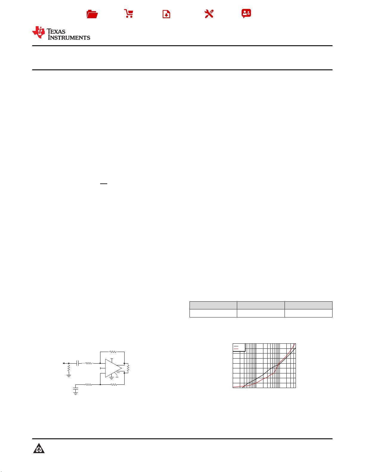
Frequency (MHz)
Distortion (dBc)
0.1 1 10 50
-140
-130
-120
-110
-100
-90
-80
-70
-60
-50
D013
HD2
HD3
C2
100 nF
Rf1
402
Rload
500
Rg1
191
C1
100 nF
Rg2
221
Rt
60.2
Output
Measurement
Point
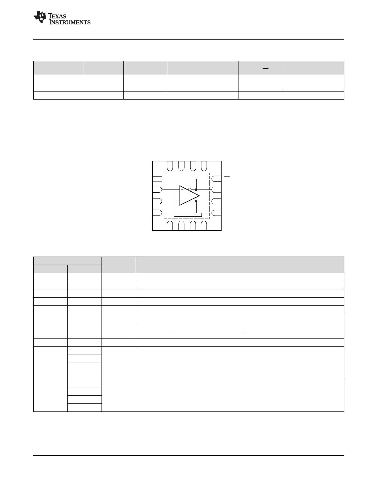
THS4541 Wideband,
Fully-Differential Amplifier
50-Input Match,
Gain of 2 V/V from Rt,
Single-Ended Source to
Differential Output
Vocm
Rf2
402
50-
Source
+
±
Vcc
+
±
Vocm
Vcc
FDA
PD
Product
Folder
Sample &
Buy
Technical
Documents
Tools &
Software
Support &
Community
An IMPORTANT NOTICE at the end of this data sheet addresses availability, warranty, changes, use in safety-critical applications,
intellectual property matters and other important disclaimers. PRODUCTION DATA.
English Data Sheet: SLOS930
THS4541-Q1
ZHCSEK0A –NOVEMBER 2015–REVISED NOVEMBER 2015
THS4541-Q1 负负轨轨输输入入、、轨轨到到轨轨输输出出、、高高精精度度、、850MHz
全全差差分分放放大大器器
1
1 特特性性
1
• 适用于汽车电子 应用
• 具有符合 AEC-Q100 标准的下列结果:
– 器件温度 1 级:-40℃ 至 +125℃ 的环境运行温
度范围
– 器件人体放电模式 (HBM) 分类等级 2
– 器件组件充电模式 (CDM) 分类等级 C6
• 完全差分放大器 (FDA) 架构
• 带宽:500MHz (G = 2V/V)
• 增益带宽产品:850MHz
• 转换率:1500V/μs
• HD
2
:10MHz 时为 –95dBc(2 V
PP
,R
L
= 500Ω)
• HD
3
:10MHz 时为 –90dBc(2 V
PP
,R
L
= 500Ω)
• 输入电压噪声:2.2nV/Hz(f > 100kHz)
• 低偏移漂移:±0.5µV/°C(典型值)
• 负轨输入 (NRI)
• 轨到轨输出 (RRO)
• Rload ≥ 50Ω 时仍可稳定运行
• 输出共模控制
• 电源:
– 单电源电压范围:2.7V 到 5.4V
– 分离电源电压范围:±1.35V 到 ±2.7V
– 静态电流:10.1mA(5V 电源)
• 断电能力:2µA(典型值)
2 应应用用
• 低功耗高性能模数转换器 (ADC) 驱动器
– SAR、ΔΣ 和流水线
• 低功耗、高性能(直流耦合或交流耦合)
– 单端到差分放大器
– 差分到差分放大器
• 差分有源滤波器
• 数模转换器 (DAC) 输出的差分互阻抗
• ADC3xxx 系列低功耗、高性能 ADC 的直流耦合或
交流耦合接口
• 与 ADA4932-1 (VQFN-16) 引脚兼容
3 说说明明
THS4541-Q1 器件是一款低功耗、电压反馈、全差分
放大器 (FDA),其具有低于负电源轨的输入共模范围以
及轨到轨输出。其设计用于低功耗数据采集系统,其中
高密度对于高性能 ADC 或 DAC 接口设计至关重要。
THS4541-Q1 器件 提供了 连接直流耦合中央接地源信
号所需的负轨输入。此负轨输入搭配轨到轨输出,只需
使用一个 2.7V 到 5.4V 的电源即可轻松将单端接地基
准双极信号源与各种逐次逼近寄存器 (SAR)、Δ-Σ 或流
水线 ADC 相连接。
THS4541-Q1 器件的额定运行温度介于 –40°C 与
+125°C 之间,并且采用 16 引脚超薄四方扁平无引线
(VQFN) 封装。
器器件件信信息息
(1)
器器件件型型号号 封封装装 封封装装尺尺寸寸((标标称称值值))
THS4541-Q1 VQFN (16) 3.00mm x 3.00mm
(1) 要了解所有可用封装,请参见数据表末尾的封装选项附录。
简简化化电电路路原原理理图图
单单端端到到差差分分增增益益为为 2,,2 V
PP
输输出出


剩余64页未读,继续阅读


评论0
最新资源