没有合适的资源?快使用搜索试试~ 我知道了~
TI-THS6226A.pdf
需积分: 5 0 下载量 69 浏览量
2022-12-06
22:45:25
上传
评论 4
收藏 2.88MB PDF 举报
温馨提示
试读
34页
TI-THS6226A.pdf
资源推荐
资源详情
资源评论
150
250
350
450
550
650
750
850
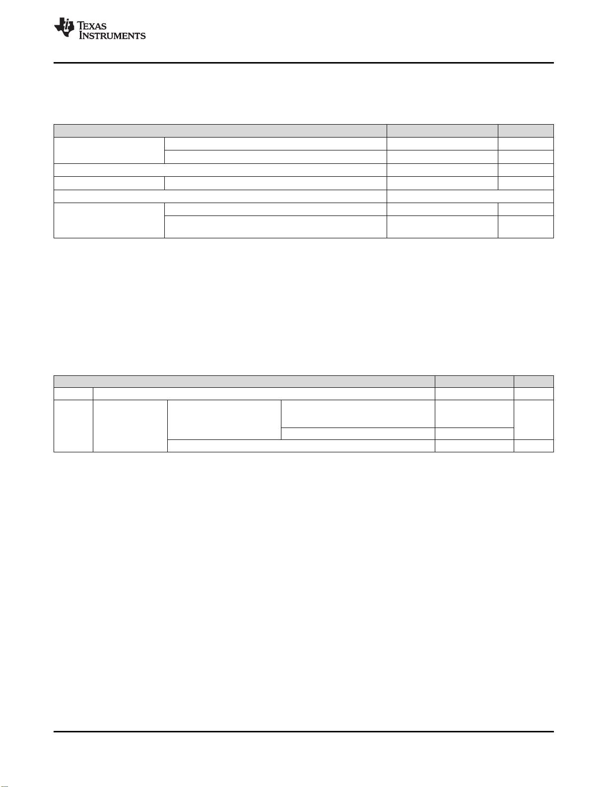
±6 ±3 0 3 6 9 12 15 18 21
Power Consumption (mW)
Tx Power (dBm)
Single Channel
Dual channel
C009
V
IN+
V
IN-
+12V
33nF
THS6226A
1:n
100kW
+12V
CLK
DATA
1 Fm
1 Fm
OUTD
OUTC
IND
INC
VLL_CD
VHH_CD
CAPL_CD
CAPH_CD
FBC
FBD
R
L
0.2 ×
n
2
R
L
Product
Folder
Sample &
Buy
Technical
Documents
Tools &
Software
Support &
Community
THS6226A
ZHCSCI0A –APRIL 2014–REVISED MAY 2014
THS6226A 门门控控 H 类类,,双双端端口口 VDSL2 线线路路驱驱动动器器
1 特特性性 3 说说明明
1
• 数字式可调节静态电流:
THS6226A 是一款双端口,H 类,电流反馈架构,差
9.4mA 至 24.8mA
分线路驱动器放大器系统,此系统非常适合于 xDSL
• 偏置电流步长:1.0mA
系统。 该器件旨在应用于超高位速率数字用户线路 2
• 独立的升压和主线路驱动器禁用
(VDSL2) 线路驱动器系统,此类系统可启用本地 DTM
• 低功率线路端接模式
信号,同时用良好线性支持高于 20.5dBm 的线路功
• 完全电容器再充电:200µs
率(在高达 8.5MHz 的频率条件下),从而支持
• 低输出电压噪声密度:
G.993.2 VDSL2 8b 传输模式。 另外,此器件还拥有
6.5nV/√Hz 输入引入电压噪声
足以支持 14.5dBm 线路功率(在高达 30MHz 的频率
• 低多音频功率比 (MTPR) 失真:
下)的中心局传输的高速度。
70dB 加上 +19.8dBm G.993.2 — 传输模式 8b
此器件的独特架构可实现极小的静态电流,同时仍然实
• -83dBc HD3(1MHz,60Ω 差分)
现超高线性度。 在全偏置条件和 1MHz 频率下,差分
• 高输出电流:(可向 60Ω 负载输送 383mA 的电
失真为 -91dBc,并在 5MHz 频率下减少为仅有 -
流)
75dBc。 对于并不需要放大器全部性能的线路长度,
• 宽输出摆幅:40V
PP
(+12V,100Ω 差分负载和一
个 1:1.4 变压器)
放大器的多种固定偏置设定值可提升节能效果。 为了
在所有的系统配置中实现更大的灵活性及节能幅度,以
• 高带宽:97MHz
0.1mA 的偏置电流步长对静态电流进行数字化调节,
• 端口至端口隔离度:1MHz 时大于 90dB
调节范围从 7.67mA 至 23mA。 对于那些希望在不传
• 电源抑制比 (PSRR):在 1MHz 频率下提供了
70dB 的良好隔离
输时节省更多电能的系统,此器件可在其线路端接模式
中使用,以保持阻抗匹配。
2 应应用用范范围围
12V 电源上的宽输出摆幅与出色的电流驱动能力相结
• 非常适合于所有的 VDSL2 传输模式
合,可实现宽动态余量,从而将失真保持在尽可能低的
• 与 ADSL,ADSL2+ 和 ADSL2++ 系统向后兼容
水平。 此器件采用超薄四方扁平无引线 (VQFN)-32
PowerPAD™ 封装。
器器件件信信息息
(1)
产产品品型型号号 封封装装 封封装装尺尺寸寸((标标称称值值))
THS6226A VQFN (32) 5.00mm x 5.00mm
(1) 如需了解所有可用封装,请见数据表末尾的可订购产品附录。
利利用用 THS6226A 的的一一个个端端口口的的典典型型 VDSL2 线线路路驱驱动动 功功耗耗与与 Tx 间间的的关关系系
器器电电路路
1
PRODUCTION DATA information is current as of publication date. Products conform to specifications per the terms of the Texas
Instruments standard warranty. Production processing does not necessarily include testing of all parameters.
English Data Sheet: SBOS643
THS6226A
ZHCSCI0A –APRIL 2014–REVISED MAY 2014
www.ti.com.cn
目目录录
7.4 Device Functional Modes........................................ 15
1 特特性性.......................................................................... 1
7.5 Programming........................................................... 16
2 应应用用范范围围................................................................... 1
8 Applications and Implementation ...................... 19
3 说说明明.......................................................................... 1
8.1 Application Information............................................ 19
4 修修订订历历史史记记录录 ........................................................... 2
8.2 Typical Application .................................................. 19
5 Pin Configuration and Functions......................... 3
8.3 Initialization Set Up ................................................ 21
6 Specifications......................................................... 5
9 Power Supply Recommendations...................... 21
6.1 Absolute Maximum Ratings ..................................... 5
10 Layout................................................................... 22
6.2 Handling Ratings....................................................... 5
10.1 Layout Guidelines ................................................. 22
6.3 Recommended Operating Conditions....................... 6
10.2 Layout Example .................................................... 23
6.4 Thermal Information.................................................. 6
11 器器件件和和文文档档支支持持 ..................................................... 24
6.5 Electrical Characteristics: V
S
= +12 V....................... 6
11.1 文档支持................................................................ 24
6.6 Timing Characteristics............................................... 8
11.2 Trademarks........................................................... 24
6.7 Typical Characteristics.............................................. 9
11.3 Electrostatic Discharge Caution............................ 24
7 Detailed Description............................................ 14
11.4 Glossary................................................................ 24
7.1 Overview ................................................................. 14
12 机机械械封封装装和和可可订订购购信信息息 .......................................... 24
7.2 Functional Block Diagram....................................... 14
7.3 Feature Description................................................. 15
4 修修订订历历史史记记录录
Changes from Original (April 2014) to Revision A Page
• Changed HBM parameter in Handling Ratings table ............................................................................................................. 5
2 Copyright © 2014, Texas Instruments Incorporated
1
2
3
4
5
6
7
8
24
23
22
21
20
19
18
17
32
9
31
10
30
11
29
12
28
13
27
14
26
15
25
16
RESET
(3)
INA
INB
CLK
DATA
INC
IND
GND
V AB
H_EN
VLL_AB
CAPL_AB
GND
V AB
S
V AB
S
CAPH_AB
VHH_AB
OUTA
FB_A
FB_B
OUTB
OUTC
FB_C
FB_D
OUTD
V CD
H_EN
VLL_CD
CAPL_CD
GND
V CD
S
V CD
S
CAPH_CD
VHH_CD
THS6226A
www.ti.com.cn
ZHCSCI0A –APRIL 2014–REVISED MAY 2014
5 Pin Configuration and Functions
RHB Package
(1)(2)
VQFN-32
(Top View)
(1) The PowerPAD is electrically isolated from all other pins and can be connected to any potential voltage range from V
S–
to V
S+
. Typically,
the PowerPAD is connected to the GND plane because this plane tends to physically be the largest and is able to dissipate the most amount
of heat.
(2) The device defaults to the disabled mode at power-up.
(3) Default is GND (internal pull-down resistor).
Copyright © 2014, Texas Instruments Incorporated 3
THS6226A
ZHCSCI0A –APRIL 2014–REVISED MAY 2014
www.ti.com.cn
Pin Functions
PIN
I/O DESCRIPTION
NO. NAME
1, 12, 29 GND — Analog ground
2 IND I Input D of amplifier CD
3 INC I Input C of amplifier CD
4 DATA I Serial interface data pin
5 CLK I Serial interface CLK pin
6 INB I Input B of amplifier AB
7 INA I Input A of amplifier AB
8 RESET I Reset the internal register to 00h (startup conditions, state machine may require resetting)
9 V
H_EN
AB I Class H mode control pin for amplifier AB
10 VLL_AB — Amplifier AB low pump supply
11 CAPL_AB — Amplifier AB negative voltage pump capacitor pin
13, 14 V
S
AB — Amplifier AB supply voltage
15 CAPH_AB — Amplifier AB positive voltage pump capacitor pin
16 VHH_AB — Amplifier AB high pump supply
17 OUTA O Output A of amplifier AB
18 FB_A I Feedback for active output impedance of amplifier AB
19 FB_B I Feedback for active output impedance of amplifier AB
20 OUTB O Output B of amplifier AB
21 OUTC O Output C of amplifier CD
22 FB_C I Feedback for active output impedance of amplifier CD
23 FB_D I Feedback for active output impedance of amplifier CD
24 OUTD O Output D of amplifier CD
25 VHH_CD — Amplifier CD high pump supply
26 CAPH_CD — Amplifier CD positive voltage pump capacitor pin
27, 28 V
S
CD — Amplifier CD supply voltage
30 CAPL_CD — Amplifier CD negative voltage pump capacitor pin
31 VLL_CD — Amplifier CD low pump supply
32 V
H_EN
CD I Class H mode control pin for amplifier CD
The PowerPAD must be connected to any internal PCB ground plane using multiple vias for good thermal
PowerPAD —
performance.
4 Copyright © 2014, Texas Instruments Incorporated
THS6226A
www.ti.com.cn
ZHCSCI0A –APRIL 2014–REVISED MAY 2014
6 Specifications
6.1 Absolute Maximum Ratings
(1)
over operating free-air temperature range (unless otherwise noted)
MIN MAX UNIT
Class AB only 16.5 V
Supply voltage, GND to V
S+
Class H only 12.8 V
Input voltage, V
I
15 V
Output current, I
O
Static dc
(2)
±100 mA
Continuous power dissipation See Thermal Information table
Maximum junction, any condition, T
J
(3)
150 °C
Temperature
Maximum junction, continuous operation, long-term reliability,
130 °C
T
J
(4)
(1) Stresses above those listed under absolute maximum ratings may cause permanent damage to the device. These are stress ratings
only, and functional operation of the device at these or any other conditions beyond those indicated under recommended operating
conditions is not implied. Exposure to absolute maximum rated conditions for extended periods may degrade device reliability.
(2) The device incorporates a PowerPAD on the underside of the chip, which functions as a heatsink and must be connected to a thermally
dissipating plane for proper power dissipation. Failure to do so may result in exceeding the maximum junction temperature, which could
permanently damage the device. See the technical brief PowerPAD™ Thermally Enhanced Package (SLMA002) for more information
about using the PowerPAD thermally-enhanced package. Under high-frequency ac operation (> 10 kHz), the short-term output current
capability is much greater than the continuous dc output current rating. This short-term output current rating is roughly 8.5 times the dc
capability, or approximately ±850 mA.
(3) The absolute maximum junction temperature under any condition is limited by the constraints of the silicon process.
(4) The absolute maximum junction temperature for continuous operation is limited by the package constraints. Operation above this
temperature may result in reduced reliability or lifetime of the device.
6.2 Handling Ratings
MIN MAX UNIT
T
stg
Storage temperature range –65 150 °C
Supply and ground pins with respect to
PowerPad: GND (pins 1, 12, 29), V
S
AB (pins –1.5 1.5
Human body model (HBM), per
kV
13, 14), V
S
CD (pins 27, 28)
Electrostatic
ANSI/ESDA/JEDEC JS-001
V
(ESD)
discharge
All other pins –2 2
Charged device model (CDM), per JEDEC specification JESD22-C101, all pins –500 500 V
Copyright © 2014, Texas Instruments Incorporated 5
剩余33页未读,继续阅读
资源评论
不觉明了
- 粉丝: 3164
- 资源: 5419
上传资源 快速赚钱
- 我的内容管理 展开
- 我的资源 快来上传第一个资源
- 我的收益 登录查看自己的收益
- 我的积分 登录查看自己的积分
- 我的C币 登录后查看C币余额
- 我的收藏
- 我的下载
- 下载帮助
最新资源
- 教学内容及补充-cha7.rar
- 设计1.ms14
- vscode-1.64.1.tar源码文件
- vscode-1.64.0.tar源码文件
- vscode-1.52.0.tar源码文件
- Music-Player +PlayerActivity+ rockplayer+ SeeJoPlayer 播放器JAVA源码
- vscode-1.46.0.tar源码文件
- 最近很火植物大战僵尸杂交版2.08苹果+安卓+PC+防闪退工具V2+修改工具+高清工具+通关存档整合包更新
- 超级好用的截图工具PixPin,可录制Gif图
- Screenshot_2024-05-21-17-06-42-64_2332cb9b27b851b548ba47a91682926c.jpg
资源上传下载、课程学习等过程中有任何疑问或建议,欢迎提出宝贵意见哦~我们会及时处理!
点击此处反馈
安全验证
文档复制为VIP权益,开通VIP直接复制
信息提交成功