TI-THS1206M.pdf
需积分: 5 18 浏览量
2022-11-27
00:06:54
上传
评论 4
收藏 1.11MB PDF 举报


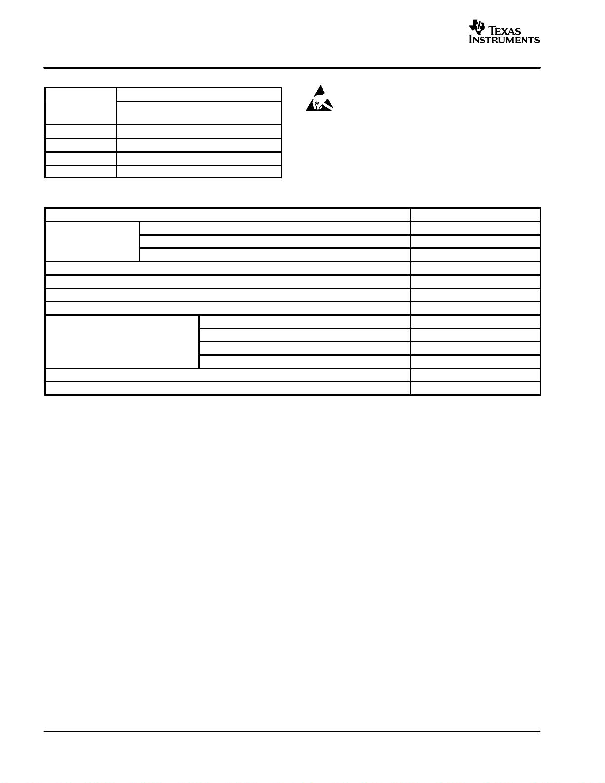
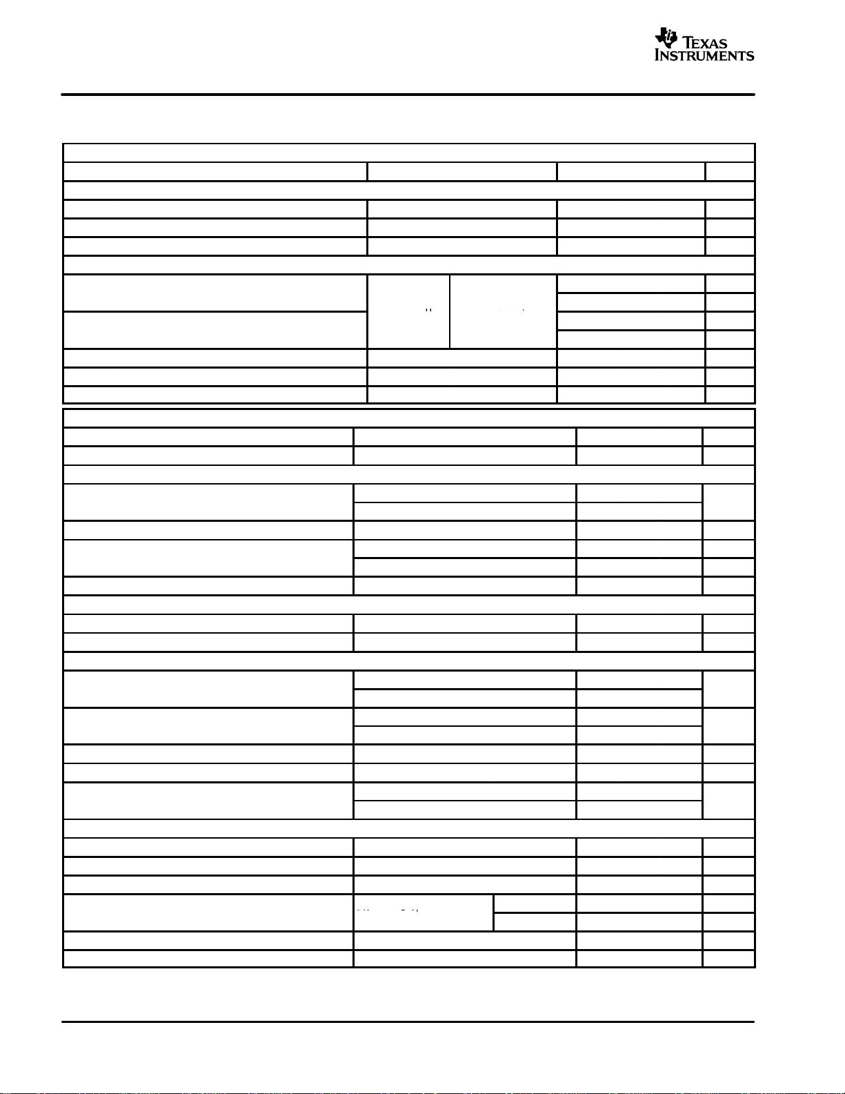
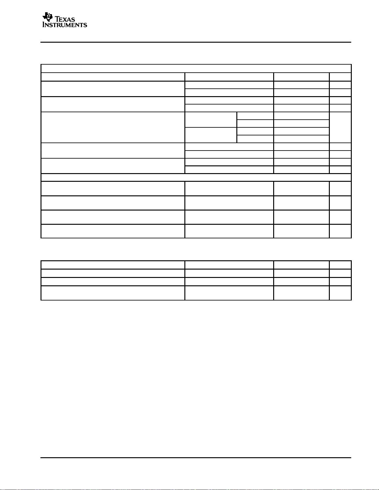
THS1206
SLAS217H – MAY 1999 – REVISED JULY 2003#
12-BIT, 4 ANALOG INPUT, 6 MSPS, SIMULTANEOUS SAMPLINGANA-
LOG-TO-DIGITAL CONVERTERS
FEATURES
D
High-Speed 6 MSPS ADC
D
4 Analog Inputs
D
Simultaneous Sampling of 4 Single-Ended
Signals or 2 Differential Signals or
Combination of Both
D
Differential Nonlinearity Error: ±1 LSB
D
Integral Nonlinearity Error: ±1.5 LSB
D
Signal-to-Noise and Distortion Ratio: 68 dB
at f
I
= 2 MHz
D
Auto-Scan Mode for 2, 3, or 4 Inputs
D
3-V or 5-V Digital Interface Compatible
D
Low Power: 216 mW Max
D
5-V Analog Single Supply Operation
D
Internal Voltage References ...50 PPM/°C
and ±5% Accuracy
D
Glueless DSP Interface
D
Parallel µC/DSP Interface
D
Integrated FIFO
D
Available in TSSOP Package
D
Pin Compatible Upgrade to THS10064
APPLICATIONS
D
Radar Applications
D
Communications
D
Control Applications
D
High-Speed DSP Front-End
D
Automotive Applications
DESCRIPTION
The THS1206 is a CMOS, low-power, 12-bit, 6 MSPS
analog-to-digital converter (ADC). The speed, resolution,
bandwidth, and single-supply operation are suited for
applications in radar, imaging, high-speed acquisition, and
communications. A multistage pipelined architecture with
output error correction logic provides for no missing codes
over the full operating temperature range. Internal control
registers are used to program the ADC into the desired
mode. The THS1206 consists of four analog inputs, which
are sampled simultaneously. These inputs can be selected
individually and configured to single-ended or differential
inputs. An integrated 16 word deep FIFO allows the
storage of data in order to take the load off of the processor
connected to the ADC. Internal reference voltages for the
ADC (1.5 V and 3.5 V) are provided.
An external reference can also be chosen to suit the dc
accuracy and temperature drift requirements of the
application. Two different conversion modes can be
selected. In single conversion mode, a single and
simultaneous conversion of up to four inputs can be
initiated by using the single conversion start signal
(CONVST
). The conversion clock in single conversion
mode is generated internally using a clock oscillator
circuit. In continuous conversion mode, an external clock
signal is applied to the CONV_CLK input of the THS1206.
The internal clock oscillator is switched off in continuous
conversion mode.
The THS1206C is characterized for operation from 0°C to
70°C while the THS1206I is characterized for operation
from –40°C to 85°C. The THS1206Q is characterized to
meet the rigorous requirements of the automotive
environment from –40°C to 125°C. The THS1206M is
characterized for operation over the full military
temperature range of –55°C to 125°C.
PRODUCT PREVIEW information concerns products in the formative or design
phase of development. Characteristic data and other specifications are design
goals. Texas Instruments reserves the right to change or discontinue these
products without notice.
Please be aware that an important notice concerning availability, standard warranty, and use in critical applications of Texas Instruments
semiconductor products and disclaimers thereto appears at the end of this data sheet.
www.ti.com
Copyright 1999 – 2003, Texas Instruments Incorporated

剩余42页未读,继续阅读
资源评论


不觉明了
- 粉丝: 3164
- 资源: 5429


最新资源
- 基于QT的地图可视化桌面系统后台数据库为MySQL5.7源码.zip
- 基于simulink的PLL锁相环系统仿真【包括模型,文档,参考文献,操作步骤】
- 基于EM-GMM模型的目标跟踪和异常行为检测matlab仿真【包括程序,注释,参考文献,操作步骤,说明文档】
- 2109010044_胡晨燕_选课管理数据库设计与实现.prj
- 帕鲁介绍的PPT备份没什么好下的
- demo1-202405
- 两种方式修改Intel网卡MAC地址
- 服务器搭建所需资源:static文件夹
- Vue02的源码学习资料
- Python 程序语言设计模式思路-行为型模式:访问者模式:在不改变被访问对象结构的情况下,定义对其元素的新操作
资源上传下载、课程学习等过程中有任何疑问或建议,欢迎提出宝贵意见哦~我们会及时处理!
点击此处反馈


