没有合适的资源?快使用搜索试试~ 我知道了~
TI-THS4524.pdf
需积分: 9 0 下载量 93 浏览量
2022-11-24
23:42:18
上传
评论 5
收藏 2.48MB PDF 举报
温馨提示
试读
69页
TI-THS4524.pdf
资源推荐
资源详情
资源评论
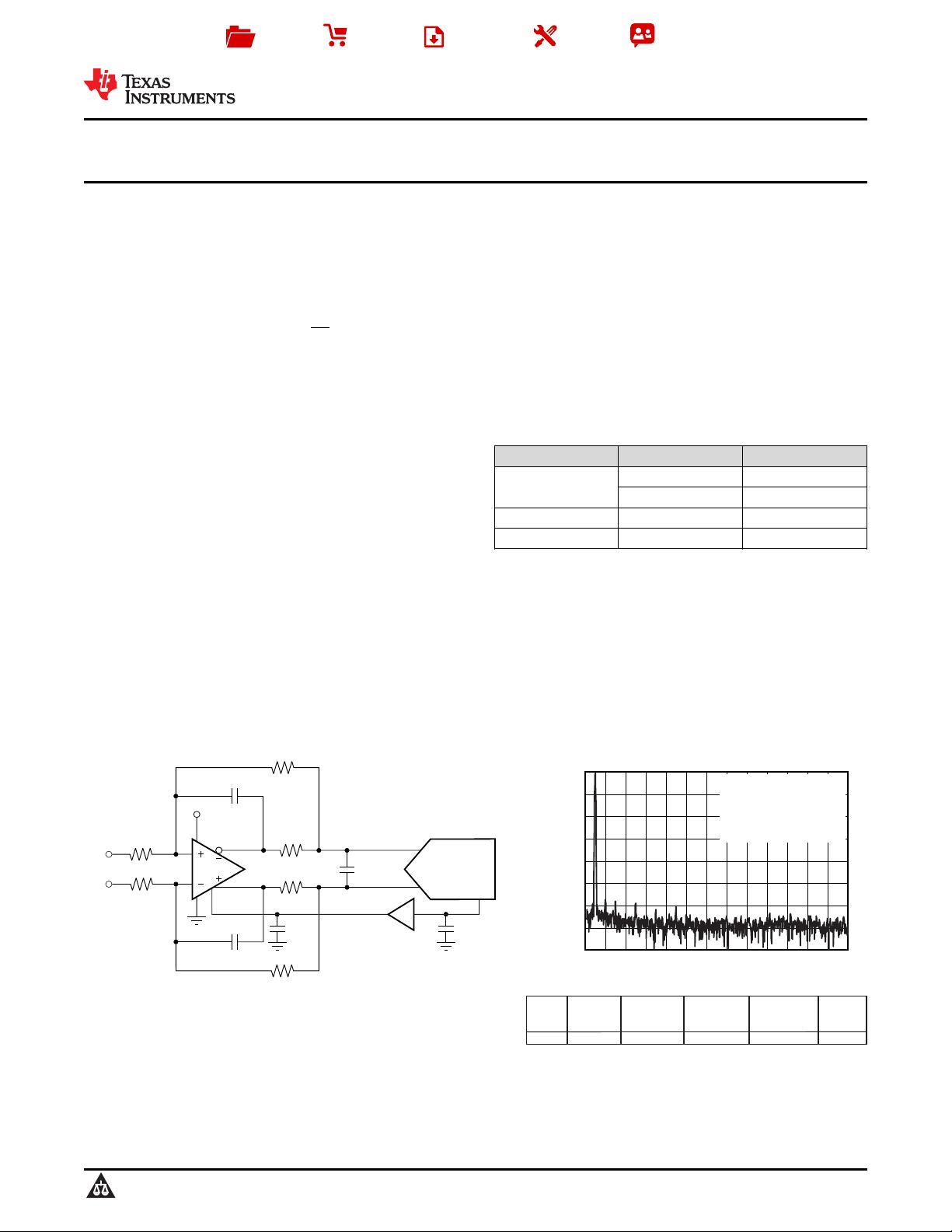
THS4521 ADS1278 (CH 1)
49.9 Ω
1 kΩ
49.9 Ω
V
OCM
V
IN+
V
IN-
5 V
V
COM
1 kΩ
1 kΩ
2.2 nF
AINN1
AINP1
0.1 Fμ
0.1 Fμ
x1
1/2
OPA2350
1.5 nF
1.5 nF
1 kΩ
0
20
40
60
80
100
120
140
-160
-
-
-
-
-
-
-
Magnitude (dBFS)
0
4
8
12
16 20
24
26
Frequency (kHz)
1-kHz FFT
G = 1
R = R = 1 k
C = 1.5 nF
V = 5 V
Load = 2.2 nF
F G
F
S
Ω
Tone
(Hz)
1 k
Signal
(dBFS)
0.50-
SNR (dBc)
109.1
THD (dBc)
107.9-
SINAD
(dBc)
105.5
SFDR
(dBc)
113.7
Product
Folder
Sample &
Buy
Technical
Documents
Tools &
Software
Support &
Community
THS4521
,
THS4522
,
THS4524
SBOS458H –DECEMBER 2008–REVISED JUNE 2015
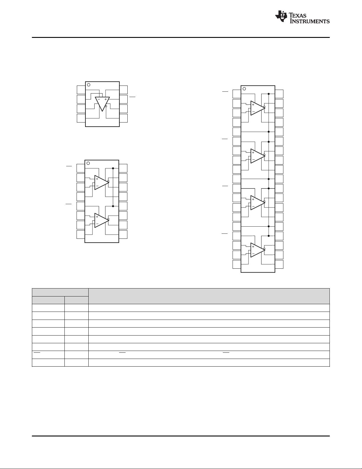
THS452x Very Low Power, Negative Rail Input, Rail-To-Rail Output, Fully Differential
Amplifier
1 Features 3 Description
The THS4521, THS4522, and THS4524 family of
1
• Fully Differential Architecture
devices are very low-power, fully differential
• Bandwidth: 145 MHz (A
V
= 1 V/V)
amplifiers with rail-to-rail output and an input
• Slew Rate: 490 V/μs
common-mode range that includes the negative rail.
These amplifiers are designed for low-power data
• HD
2
: –133 dBc at 10 kHz (1 V
RMS
, R
L
= 1 kΩ)
acquisition systems and high-density applications
• HD
3
: –141 dBc at 10 kHz (1 V
RMS
, R
L
= 1 kΩ)
where power dissipation is a critical parameter, and
• Input Voltage Noise: 4.6 nV/√Hz (f = 100 kHz)
provide exceptional performance in audio
applications.
• THD+N: –112dBc (0.00025%) at 1 kHz (22-kHz
BW, G = 1, 5 V
PP
)
The family includes single FDA (THS4521), dual FDA
• Open-Loop Gain: 119 dB (DC)
(THS4522), and quad FDA (THS4524) versions.
• NRI—Negative Rail Input
Device Information
(1)
• RRO—Rail-to-Rail Output
PART NUMBER PACKAGE BODY SIZE (NOM)
• Output Common-Mode Control (with Low Offset)
SOIC (8) 4.90 mm × 3.91 mm
THS4521
• Power Supply:
VSSOP (8) 3.00 mm × 3.00 mm
– Voltage: +2.5 V (±1.25 V) to +5.5 V (±2.75 V)
THS4522 TSSOP (16) 5.00 mm × 4.40 mm
– Current: 1.14 mA/ch
THS4524 TSSOP (38) 9.70 mm × 4.40 mm
• Power-Down Capability: 20 μA (typical)
(1) For all available packages, see the package option addendum
at the end of the datasheet.
2 Applications
• Low-Power SAR and ΔΣ ADC Drivers
• Low-Power Differential Drivers
• Low-Power Differential Signal Conditioning
• Low-Power, High-Performance Differential Audio
Amplifiers
THS4521 and ADS1278 Combined Performance
For more information on this circuit, view SBAU197.
1
An IMPORTANT NOTICE at the end of this data sheet addresses availability, warranty, changes, use in safety-critical applications,
intellectual property matters and other important disclaimers. PRODUCTION DATA.
THS4521
,
THS4522
,
THS4524
SBOS458H –DECEMBER 2008–REVISED JUNE 2015
www.ti.com
Table of Contents
8.3 Feature Description................................................. 25
1 Features.................................................................. 1
8.4 Device Functional Modes........................................ 34
2 Applications ........................................................... 1
8.5 Programming........................................................... 40
3 Description ............................................................. 1
9 Application and Implementation ........................ 41
4 Revision History..................................................... 2
9.1 Application Information............................................ 41
5 Device Comparison Table..................................... 3
9.2 Typical Applications ............................................... 41
6 Pin Configuration and Functions......................... 4
10 Power Supply Recommendations ..................... 51
7 Specifications ......................................................... 7
11 Layout................................................................... 51
7.1 Absolute Maximum Ratings ...................................... 7
11.1 Layout Guidelines ................................................. 51
7.2 ESD Ratings ............................................................ 7
11.2 Layout Example .................................................... 52
7.3 Recommended Operating Conditions....................... 7
12 Device and Documentation Support ................. 53
7.4 Thermal Information.................................................. 7
12.1 Device Support...................................................... 53
7.5 Electrical Characteristics: V
S+
– V
S–
= 3.3 V ............ 8
12.2 Related Links ........................................................ 53
7.6 Electrical Characteristics: V
S+
– V
S–
= 5 V ............. 10
12.3 Community Resources.......................................... 53
7.7 Typical Characteristics............................................ 12
12.4 Trademarks........................................................... 53
7.8 Typical Characteristics: V
S+
– V
S–
= 3.3 V.............. 14
12.5 Electrostatic Discharge Caution............................ 53
7.9 Typical Characteristics: 5 V .................................... 19
12.6 Glossary................................................................ 53
8 Detailed Description ............................................ 24
13 Mechanical, Packaging, and Orderable
8.1 Overview ................................................................. 24
Information ........................................................... 53
8.2 Functional Block Diagram ....................................... 25
4 Revision History
NOTE: Page numbers for previous revisions may differ from page numbers in the current version.
Changes from Revision G (December 2014) to Revision H Page
• Changed capacitor units in front page diagram from mF to µF (typo) ................................................................................... 1
• Changed RF and RG unit in front page FFT plot from kW to kΩ (typo)................................................................................. 1
• Changed Absolute Maximum Ratings minimum storage temperature value from 65 to –65 (typo) ..................................... 7
• Added Community Resources section ................................................................................................................................. 53
Changes from Revision F (September 2011) to Revision G Page
• Added Pin Configuration and Functions section, ESD Ratings table, Feature Description section, Device Functional
Modes, Application and Implementation section, Power Supply Recommendations section, Layout section, Device
and Documentation Support section, and Mechanical, Packaging, and Orderable Information section .............................. 1
Changes from Revision E (December 2010) to Revision F Page
• Changed Input Offset Current values in 3.3 V Electrical Characteristics............................................................................... 8
• Changed Input Offset Current Drift values in 3.3 V Electrical Characteristics ....................................................................... 8
• Changed Input Offset Current values in 5 V Electrical Characteristics................................................................................ 11
• Changed Input Offset Current Drift values in 5 V Electrical Characteristics ........................................................................ 11
• Changed R41 and R42 in Figure 79..................................................................................................................................... 42
Changes from Revision D (August 2010) to Revision E Page
• Changed test level indication for 5-V input offset voltage drift from B to C.......................................................................... 10
2 Submit Documentation Feedback Copyright © 2008–2015, Texas Instruments Incorporated
Product Folder Links: THS4521 THS4522 THS4524
THS4521
,
THS4522
,
THS4524
www.ti.com
SBOS458H –DECEMBER 2008–REVISED JUNE 2015
5 Device Comparison Table
These fully differential amplifiers feature accurate output common-mode control that allows for dc-coupling when
driving analog-to-digital converters (ADCs). This control, coupled with an input common-mode range below the
negative rail as well as rail-to-rail output, allows for easy interfacing between single-ended, ground-referenced
signal sources. Additionally, these devices are ideally suited for driving both successive-approximation register
(SAR) and delta-sigma (ΔΣ) ADCs using only a single +2.5V to +5V and ground power supply.
The THS4521, THS4522, and THS4524 family of fully differential amplifiers is characterized for operation over
the full industrial temperature range from –40°C to +85°C. Table 1 shows a comparison of the THS4521 device
to similar TI devices.
Table 1. THS4521 Device Comparison
BW I
Q
THD (dBc) V
N
DUAL PART
DEVICE (MHz) (mA) AT 100 kHz (nV/√Hz) RAIL-TO-RAIL NUMBERS
THS4531 36 0.25 –104 10.0 Neg In, Out —
THS4521 145 0.95 –102 4.6 Neg In, Out THS4522
THS4520 620 14.2 –107 2.0 Out —
THS4541 850 10.1 –137 2.2 Neg In, Out —
Copyright © 2008–2015, Texas Instruments Incorporated Submit Documentation Feedback 3
Product Folder Links: THS4521 THS4522 THS4524
13
14
15
16
17
18
19
26
25
24
23
22
21
20
V
OUT3+
V
S3+
V
S-
V
OUT4-
V
OUT4+
V
S4+
V
IN3+
V
IN3-
V
OCM3
PD
4
V
IN4+
V
IN4-
V
OCM4
9
10
11
12
30
29
28
27
V
S2+
V
S-
V
OUT3-
PD
2
PD
3
1
2
3
4
5
6
7
8
38
37
36
35
34
33
32
31
V
S-
V
OUT1-
V
OUT1+
V
S1+
V
S-
V
OUT2-
V
OUT2+
PD
1
V
IN1+
V
IN1-
V
OCM1
V
S-
V
IN2+
V
IN2-
V
OCM2
V
S-
V
S-
V
S-
V
S-
V
S-
1
2
3
4
5
6
7
8
16
15
14
13
12
11
10
9
V
S-
V
OUT1-
V
OUT1+
V
S1+
V
S-
V
OUT2-
V
OUT2+
V
S2+
PD
1
V
IN1+
V
IN1-
V
OCM1
PD
2
V
IN2+
V
IN2-
V
OCM2
1
2
3
4
8
7
6
5
V
IN+
PD
V
S-
V
OUT-
V
IN-
V
OCM
V
S+
V
OUT+
THS4521
,
THS4522
,
THS4524
SBOS458H –DECEMBER 2008 –REVISED JUNE 2015
www.ti.com
6 Pin Configuration and Functions
THS4521 D and DGK Package
THS4524 DBT Package
8-Pin SOIC and VSSOP
38-Pin TSSOP
Top View
Top View
THS4522 PW Package
16-Pin TSSOP
Top View
Pin Functions: THS4521
PIN
DESCRIPTION
NAME NO.
V
IN–
1 Inverting amplifier input
V
OCM
2 Common-mode voltage input
V
S+
3 Amplifier positive power-supply input
V
OUT+
4 Noninverting amplifier output
V
OUT–
5 Inverting amplifier output
V
S–
6 Amplifier negative power-supply input. Note that V
S–
is tied together on multi-channel devices.
PD 7 Power down. PD = logic low puts device into low-power mode. PD = logic high or open for normal operation.
V
IN+
8 Noninverting amplifier input
4 Submit Documentation Feedback Copyright © 2008–2015, Texas Instruments Incorporated
Product Folder Links: THS4521 THS4522 THS4524
THS4521
,
THS4522
,
THS4524
www.ti.com
SBOS458H –DECEMBER 2008–REVISED JUNE 2015
Pin Functions: THS4522
PIN
DESCRIPTION
NAME NO.
PD
1
1 Power down 1. PD = logic low puts device into low-power mode. PD = logic high or open for normal operation.
V
IN1+
2 Noninverting amplifier 1 input
V
IN1–
3 Inverting amplifier 1 input
V
OCM1
4 Common-mode voltage input 1
PD
2
5 Power down 2. PD = logic low puts device into low-power mode. PD = logic high or open for normal operation.
V
IN2+
6 Noninverting amplifier 2 input
V
IN2–
7 Inverting amplifier 2 input
V
OCM2
8 Common-mode voltage input 2
V
S+2
9 Amplifier 2 positive power-supply input
V
OUT2+
10 Noninverting amplifier 2 output
V
OUT2–
11 Inverting amplifier 2 output
V
S–
12 Negative power-supply input. Note that V
S–
is tied together on multi-channel devices.
V
S+1
13 Amplifier 1 positive power-supply input
V
OUT1+
14 Noninverting amplifier 1 output
V
OUT1–
15 Inverting amplifier 1 output
V
S–
16 Negative power-supply input. Note that V
S–
is tied together on multi-channel devices.
Copyright © 2008–2015, Texas Instruments Incorporated Submit Documentation Feedback 5
Product Folder Links: THS4521 THS4522 THS4524
剩余68页未读,继续阅读
资源评论
不觉明了
- 粉丝: 3118
- 资源: 5348
上传资源 快速赚钱
- 我的内容管理 展开
- 我的资源 快来上传第一个资源
- 我的收益 登录查看自己的收益
- 我的积分 登录查看自己的积分
- 我的C币 登录后查看C币余额
- 我的收藏
- 我的下载
- 下载帮助
安全验证
文档复制为VIP权益,开通VIP直接复制
信息提交成功