TI-THS6072.pdf
需积分: 5 4 浏览量
2022-12-06
22:45:47
上传
评论 4
收藏 1.15MB PDF 举报


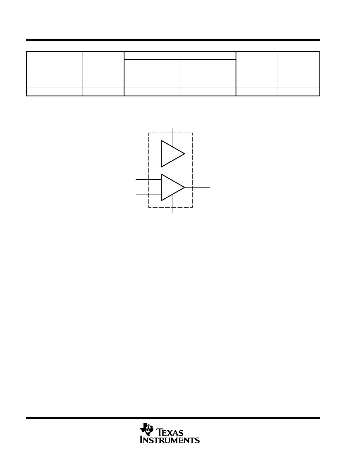
THS6072
LOW-POWER ADSL DIFFERENTIAL RECEIVER
SLOS290B – FEBRUARY 2000 – REVISED JUNE 2001
1
POST OFFICE BOX 655303 • DALLAS, TEXAS 75265
D
ADSL Differential Receiver
– Ideal for Central Office or Remote
Terminal Applications
D
Low 3.4 mA Per Channel Quiescent Current
D
10 nV/√Hz Voltage Noise
D
Very Low Distortion
– THD = –79 dBc (f = 1 MHz, R
L
= 1 kΩ)
D
High Speed
– 175 MHz Bandwidth (–3 dB, G = 1)
– 230 V/µs Slew Rate
D
High Output Drive, I
O
= 85 mA (typ)
D
Wide Range of Power Supplies
– V
CC
= ±5 V to ±15 V
D
Available in Standard SOIC or MSOP
PowerPAD Package
D
Evaluation Module Available
description
The THS6072 is a high-speed, low-power differential receiver designed for ADSL communication systems. Its
low 3.4-mA per channel quiescent current reduces power to half that of other ADSL receivers making it ideal
for low power ADSL applications. This receiver operates with a very low distortion of –79 dBc
(f = 1 MHz, R
L
= 1 kΩ). The THS6072 is a voltage feedback amplifier offering a high 175-MHz bandwidth and
230-V/µs slew rate and is unity gain stable. It operates over a wide range of power supply voltages including
±4.5 V to ±15 V. This device is available in a standard SOIC or MSOP PowerPAD package.
HIGH-SPEED xDSL LINE DRIVER/RECEIVER FAMILY
DEVICE
DRIVER RECEIVER 5 V ±5 V ±15 V DESCRIPTION
THS6002
•
• • • 500-mA differential line driver and receiver
THS6012 • • • 500-mA differential line driver
THS6022 • • • 250-mA differential line driver
THS6032 • • • 500-mA low-power ADSL central-office line driver
THS6042/3 • • • 350-mA, ±12 V ADSL CPE Line Drivers
THS6052/3 • • • 100-mA, ±12 V ADSL CPE Line Drivers
THS6062 • • • • Low-noise ADSL receiver
THS6072 • • • Low-power ADSL receiver
THS6092/3 • • • 200-mA, ±12 V ADSL CPE Line Drivers
THS7002 • • • Low-noise programmable-gain ADSL receiver
PowerPAD is a trademark of Texas Instruments.
Copyright 2001, Texas Instruments Incorporated
PRODUCTION DATA information is current as of publication date.
Products conform to specifications per the terms of Texas Instruments
standard warranty. Production processing does not necessarily include
testing of all parameters.
Please be aware that an important notice concerning availability, standard warranty, and use in critical applications of
Texas Instruments semiconductor products and disclaimers thereto appears at the end of this data sheet.
Cross Section View Showing
PowerPAD Option (DGN)
1
2
3
4
8
7
6
5
1OUT
1IN–
1IN+
V
CC–
V
CC
+
2OUT
2IN–
2IN+
THS6072
D OR DGN PACKAGE
(TOP VIEW)
CAUTION: The THS6072 provides ESD protection circuitry. However, permanent damage can still occur if this device is subjected
to high-energy electrostatic discharges. Proper ESD precautions are recommended to avoid any performance degradation or loss
of functionality.
剩余30页未读,继续阅读
资源评论


