没有合适的资源?快使用搜索试试~ 我知道了~
TI-THS6214.pdf
需积分: 5 0 下载量 169 浏览量
2022-12-06
22:46:28
上传
评论 4
收藏 2.57MB PDF 举报
温馨提示
试读
50页
TI-THS6214.pdf
资源推荐
资源详情
资源评论
12 V
12 V
R
S
R
S
R
G
R
T
R
T
R
F
R
P
R
P
R
F
I
ADJ
100 W
Product
Folder
Order
Now
Technical
Documents
Tools &
Software
Support &
Community
An IMPORTANT NOTICE at the end of this data sheet addresses availability, warranty, changes, use in safety-critical applications,
intellectual property matters and other important disclaimers. PRODUCTION DATA.
THS6214
SBOS431A –MAY 2009–REVISED MARCH 2017
THS6214 Dual-Port, Differential, VDSL2 Line Driver Amplifiers
1
1 Features
1
• Low Power Consumption:
– Full Bias Mode: 21 mA per Port
– Mid Bias Mode: 16.2 mA per Port
– Low Bias Mode: 11.2 mA per Port
– Low-Power Shutdown Mode
– I
ADJ
Pin for Variable Bias
• Low Noise:
– Voltage Noise: 2.7 nV/√Hz
– Inverting Current Noise: 17 pA/√Hz
– Noninverting Current Noise: 1.2 pA/√Hz
• Low MTPR Distortion:
– 70 dB with 20.5 dBm G.993.2—Profile 8b
• –93 dBc HD3 (1 MHz, 100-Ω Differential)
• High Output Current: > 416 mA (25-Ω Load)
• Wide Output Swing: 43.2 V
PP
(±12 V, 100-Ω
Differential Load)
• Wide Bandwidth: 150 MHz (G
DIFF
= 10 V/V)
• PSRR: 50 dB at 1 MHz for Good Isolation
• Wide Power-Supply Range: 10 V to 28 V
2 Applications
• Ideal For VDSL2 Systems
• Backwards-Compatible with ADSL, ADSL2+,
ADSL2++ Systems
• Broadband Power Line Communications
3 Description
The THS6214 is a dual-port, current-feedback
architecture, differential line driver amplifier system
ideal for xDSL systems. The device is targeted for
use in very-high-bit-rate digital subscriber line 2
(VDSL2) line driver systems that enable greater than
14.5-dBm line power, supporting the G.993.2 VDSL2
17a profile. The device is also fast enough to support
central-office transmissions of 14.5-dBm line power
up to 30 MHz. The device is also targeted for use as
a broadband or wideband power line communications
(PLC) amplifier for line driver applications.
The unique architecture of the THS6214 uses
minimal quiescent current and still achieves very high
linearity. Differential distortion, under full bias
conditions, is –93 dBc at 1 MHz and reduces to only
–73 dBc at 10 MHz. Fixed multiple bias settings of
the amplifiers allow for enhanced power savings for
line lengths where the full performance of the
amplifier is not required. To allow for even more
flexibility and power savings, an adjustable current
pin (I
ADJ
) is available to further lower the bias
currents.
The wide output swing of 43.2 V
PP
(100-Ω differential
load) with ± 12-V power supplies, coupled with over
416-mA current drive (25-Ω load), allows for wide
dynamic headroom, keeping distortion minimal.
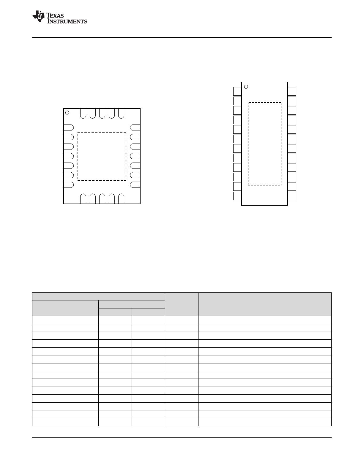
The THS6214 is available in a VQFN-24 or a
HTSSOP-24 PowerPAD™ package.
Device Information
(1)
PART NUMBER PACKAGE BODY SIZE (NOM)
THS6214
VQFN (24) 5.00 mm × 4.00 mm
HTSSOP (24) 7.80 mm × 4.40 mm
(1) For all available packages, see the orderable addendum at
the end of the data sheet.
Typical VDSL2 Line Driver Circuit Using One Port of the THS6214
2
THS6214
SBOS431A –MAY 2009–REVISED MARCH 2017
www.ti.com
Product Folder Links: THS6214
Submit Documentation Feedback Copyright © 2009–2017, Texas Instruments Incorporated
Table of Contents
1 Features.................................................................. 1
2 Applications ........................................................... 1
3 Description ............................................................. 1
4 Revision History..................................................... 2
5 Pin Configuration and Functions......................... 3
6 Specifications......................................................... 4
6.1 Absolute Maximum Ratings ...................................... 4
6.2 ESD Ratings.............................................................. 5
6.3 Recommended Operating Conditions....................... 5
6.4 Thermal Information.................................................. 5
6.5 Electrical Characteristics: V
S
= ±12 V....................... 6
6.6 Electrical Characteristics: V
S
= ±6 V......................... 8
6.7 Timing Requirements.............................................. 10
6.8 Typical Characteristics: V
S
= ±12 V, Full Bias ........ 11
6.9 Typical Characteristics: V
S
= ±12 V, Mid Bias ........ 14
6.10 Typical Characteristics: V
S
= ±12 V, Low Bias ..... 16
6.11 Typical Characteristics: V
S
= ±6 V, Full Bias ........ 18
6.12 Typical Characteristics: V
S
= ±6 V, Mid Bias ........ 21
6.13 Typical Characteristics: V
S
= ±6 V, Low Bias ....... 23
7 Detailed Description............................................ 25
7.1 Overview ................................................................. 25
7.2 Functional Block Diagram ....................................... 25
7.3 Feature Description................................................. 25
7.4 Device Functional Modes........................................ 28
8 Application and Implementation ........................ 29
8.1 Application Information............................................ 29
8.2 Typical Applications ................................................ 29
9 Power Supply Recommendations...................... 35
10 Layout................................................................... 36
10.1 Board Layout Guidelines....................................... 36
10.2 Layout Example .................................................... 37
11 Device and Documentation Support ................. 38
11.1 Receiving Notification of Documentation Updates 38
11.2 Community Resources.......................................... 38
11.3 Trademarks........................................................... 38
11.4 Electrostatic Discharge Caution............................ 38
11.5 Glossary................................................................ 38
12 Mechanical, Packaging, and Orderable
Information ........................................................... 38
4 Revision History
Changes from Original (May 2009) to Revision A Page
• Added Device Information table, Pin Functions table, ESD Ratings table, Recommended Operating Conditions
table, Thermal Information table, Timing Requirements table, Overview section, Functional Block Diagram section,
Feature Description section, Device Functional Modes section, Application and Implementation section, Power
Supply Recommendations section, Layout section, Device and Documentation Support section, and Mechanical,
Packaging, and Orderable Information section ...................................................................................................................... 1
• Added last Applications bullet ................................................................................................................................................ 1
• Added last sentence to first paragraph of Description section .............................................................................................. 1
• Changed QFN to VQFN and TSSOP to HTSSOP throughout document ............................................................................. 1
• Deleted Ordering Information table ....................................................................................................................................... 3
• Deleted Dissipation Ratings table .......................................................................................................................................... 5
• Changed second paragraph of Distortion Performance section for clarity........................................................................... 26
D1 IN+
D2 IN+
GND
I
ADJ
NC
D3 IN+
D2 FB
D2 OUT
NC
D3 OUT
D3 FB
D4 FB
1
2
3
4
5
6
18
17
16
15
14
13
PowerPAD
BIAS-2/D1D2
24
23
22
21
20
19
D4 IN+
BIAS-1/D1D2
BIAS-2/D3D4
V
S-
BIAS-1/D3D4
V
S+
V
S-
D1 OUT
V
S+
D1 FB
D4 OUT
7
8
9
10
11
12
V
S-
BIAS-1/D1D2
BIAS-2/D1D2
D1 IN+
D2 IN+
GND
I
ADJ
D3 IN+
D4 IN+
BIAS-2/D3D4
BIAS-1/D3D4
V
S-
V
S+
D1 OUT
D1 FB
D2 FB
D2 OUT
NC
NC
D3 OUT
D3 FB
D4 FB
D4 OUT
V
S+
1
2
3
4
5
6
7
8
9
10
11
12
24
23
22
21
20
19
18
17
16
15
14
13
PowerPAD
3
THS6214
www.ti.com
SBOS431A –MAY 2009–REVISED MARCH 2017
Product Folder Links: THS6214
Submit Documentation FeedbackCopyright © 2009–2017, Texas Instruments Incorporated
5 Pin Configuration and Functions
RHF Package
24-Pin VQFN
Top View
PWP Package
24-Pin HTSSOP
Top View
(1) The PowerPAD is electrically isolated from all other pins and can be connected to any potential voltage range from
V
S–
to V
S+
. Typically, the PowerPAD is connected to the GND plane because this plane tends to physically be the
largest and is able to dissipate the most amount of heat.
(2) The THS6214 defaults to the shutdown (disable) state if no signal is present on the bias pins.
(3) The GND pin range is from V
S–
to (V
S+
– 5 V).
NOTE: NC = no connection.
(1) The THS6214 defaults to the shutdown (disable) state if no signal is present on the bias pins.
Pin Functions
(1)
PIN
I/O DESCRIPTION
NAME
NO.
RHF PWP
BIAS-1/D1D2 23 2 I Bias mode parallel control for port A, LSB
BIAS-1/D3D4 9 11 I Bias mode parallel control for port B, LSB
BIAS-2/D1D2 24 3 I Bias mode parallel control for port A, MSB
BIAS-2/D3D4 8 10 I Bias mode parallel control for port B, MSB
D1 FB 19 22 I Amplifier D1 inverting input
D2 FB 18 21 I Amplifier D2 inverting input
D3 FB 14 16 I Amplifier D3 inverting input
D4 FB 13 15 I Amplifier D4 inverting input
D1 IN+ 1 4 I Amplifier D1 noninverting input
D2 IN+ 2 5 I Amplifier D2 noninverting input
D3 IN+ 6 8 I Amplifier D3 noninverting input
D4 IN+ 7 9 I Amplifier D4 noninverting input
D1 OUT 20 23 O Amplifier D1 output
D2 OUT 17 20 O Amplifier D2 output
4
THS6214
SBOS431A –MAY 2009–REVISED MARCH 2017
www.ti.com
Product Folder Links: THS6214
Submit Documentation Feedback Copyright © 2009–2017, Texas Instruments Incorporated
Pin Functions
(1)
(continued)
PIN
I/O DESCRIPTION
NAME
NO.
RHF PWP
(2) The GND pin range is from V
S–
to (V
S+
– 5 V).
D3 OUT 15 17 O Amplifier D3 output
D4 OUT 12 14 O Amplifier D4 output
GND
(2)
3 6 I/O Control pin ground reference
I
ADJ
4 7 I/O Bias current adjustment pin
NC 5, 16 18, 19 — No internal connection
V
S–
10, 22 1, 12 I/O Negative power-supply connection
V
S+
11, 21 11, 24 I/O Positive power-supply connection
Table 1. BIAS-1, BIAS-2 Logic Table
BIAS-1 BIAS-0 FUNCTION DESCRITPION
0 0 Full bias mode (100%) Amplifiers on with lowest distortion possible (default state)
1 0 Mid bias mode (75%) Amplifiers on with power savings and a reduction in distortion performance
0 1 Low bias mode (50%)
Amplifiers on with enhanced power savings and a reduction of overall
performance
1 1 Shutdown mode Amplifiers off and output has high impedance
(1) Stresses beyond those listed under Absolute Maximum Ratings may cause permanent damage to the device. These are stress ratings
only, which do not imply functional operation of the device at these or any other conditions beyond those indicated under Recommended
Operating Conditions. Exposure to absolute-maximum-rated conditions for extended periods may affect device reliability.
(2) The THS6214 incorporates a PowerPAD on the underside of the chip. This pad functions as a heatsink and must be connected to a
thermally dissipating plane for proper power dissipation. Failure to do so may result in exceeding the maximum junction temperature,
which can permanently damage the device. See PowerPAD™ Thermally Enhanced Package (SLMA002) for more information about
using the PowerPAD thermally-enhanced package. Under high-frequency ac operation (greater than 10 kHz), the short-term output
current capability is much greater than the continuous dc output current rating. This short-term output current rating is approximately 8.5
times the dc capability, or approximately ±850 mA.
(3) The absolute maximum junction temperature under any condition is limited by the constraints of the silicon process.
(4) The absolute maximum junction temperature for continuous operation is limited by the package constraints. Operation above this
temperature may result in reduced reliability and/or lifetime of the device.
6 Specifications
6.1 Absolute Maximum Ratings
over operating free-air temperature range (unless otherwise noted)
(1)
MIN MAX UNIT
Supply voltage, V
S–
to V
S+
28 V
Input voltage, V
I
±V
S
V
Differential input voltage, V
ID
±2 V
Output current, I
O
Static dc
(2)
±500 mA
Continuous power dissipation See Thermal Information
Maximum junction temperature, T
J
Under any condition
(3)
150
°C
Continuous operation, long-term reliability
(4)
,
RHF package only
130
Continuous operation, long-term reliability
(4)
,
PWP package only
140
Storage temperature, T
stg
–65 150 °C
5
THS6214
www.ti.com
SBOS431A –MAY 2009–REVISED MARCH 2017
Product Folder Links: THS6214
Submit Documentation FeedbackCopyright © 2009–2017, Texas Instruments Incorporated
(1) JEDEC document JEP155 states that 500-V HBM allows safe manufacturing with a standard ESD control process.
(2) JEDEC document JEP157 states that 250-V CDM allows safe manufacturing with a standard ESD control process.
6.2 ESD Ratings
VALUE UNIT
V
(ESD)
Electrostatic discharge
Human-body model (HBM), per ANSI/ESDA/JEDEC JS-001
(1)
±2000
VCharged-device model (CDM), per JEDEC specification JESD22-C101
(2)
±500
Machine model (MM) ±100
6.3 Recommended Operating Conditions
over operating free-air temperature range (unless otherwise noted)
MIN NOM MAX UNIT
V
S
Supply voltage, V
S–
to V
S+
10 28 V
T
J
Operating junction temperature 130 °C
T
A
Ambient operating air temperature 25 85 °C
(1) For more information about traditional and new thermal metrics, see the Semiconductor and IC Package Thermal Metrics application
report.
6.4 Thermal Information
THERMAL METRIC
(1)
THS6214
UNITRHF (VQFN) PWP (HTSSOP)
24 PINS 24 PINS
R
θJA
Junction-to-ambient thermal resistance 33.2 35.7 °C/W
R
θJC(top)
Junction-to-case (top) thermal resistance 31.7 22.9 °C/W
R
θJB
Junction-to-board thermal resistance 11.3 10.1 °C/W
ψ
JT
Junction-to-top characterization parameter 0.4 0.4 °C/W
ψ
JB
Junction-to-board characterization parameter 11.3 10.3 °C/W
R
θJC(bot)
Junction-to-case (bottom) thermal resistance 3.9 1.7 °C/W
剩余49页未读,继续阅读
资源评论
不觉明了
- 粉丝: 3164
- 资源: 5429
上传资源 快速赚钱
- 我的内容管理 展开
- 我的资源 快来上传第一个资源
- 我的收益 登录查看自己的收益
- 我的积分 登录查看自己的积分
- 我的C币 登录后查看C币余额
- 我的收藏
- 我的下载
- 下载帮助
安全验证
文档复制为VIP权益,开通VIP直接复制
信息提交成功