没有合适的资源?快使用搜索试试~ 我知道了~
TI-THS7314.pdf
需积分: 5 0 下载量 55 浏览量
2022-12-04
00:12:43
上传
评论 4
收藏 1.29MB PDF 举报
温馨提示
试读
32页
TI-THS7314.pdf
资源推荐
资源详情
资源评论
5
8
7
6
V
S+
GND
CH.2IN
CH.3IN
CH.1IN
CH.3OUT
CH.2OUT
CH.1OUT
DAC/
Encoder
(THS8200)
1
2
3
4
CVBS
Y’
C’
CVBS
Out
75 W
Y’
Out
75 W
C’
Out
75 W
3.3V
3.3V
75 W
75 W
SDTV
CVBS
S-Video Y’
S-VideoC’
480i/576i
Y’P’ P’
G’B’R’
B R
75 W
S-Video
R
R
R
THS7314
THS7314
www.ti.com
SLOS513A –DECEMBER 2006– REVISED MARCH 2011
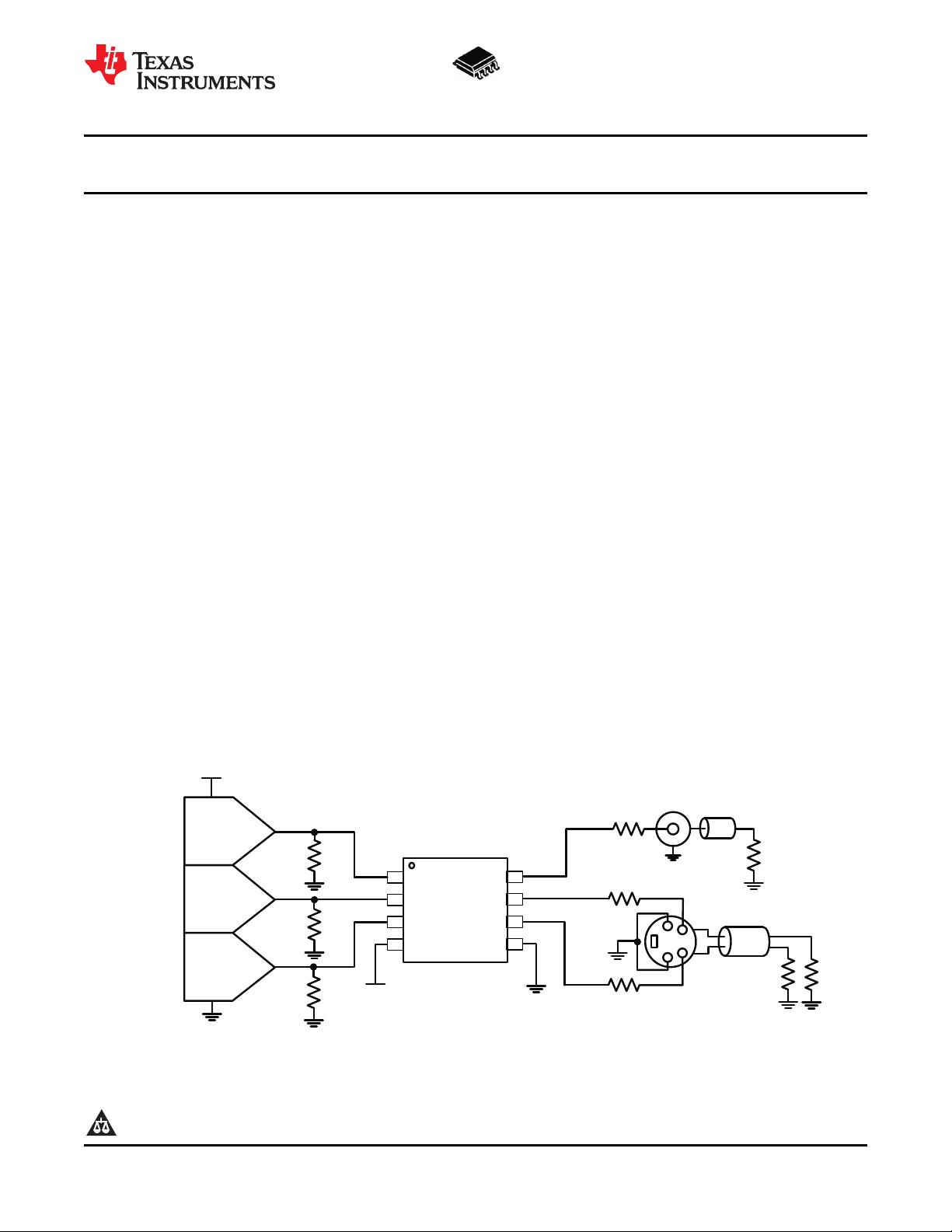
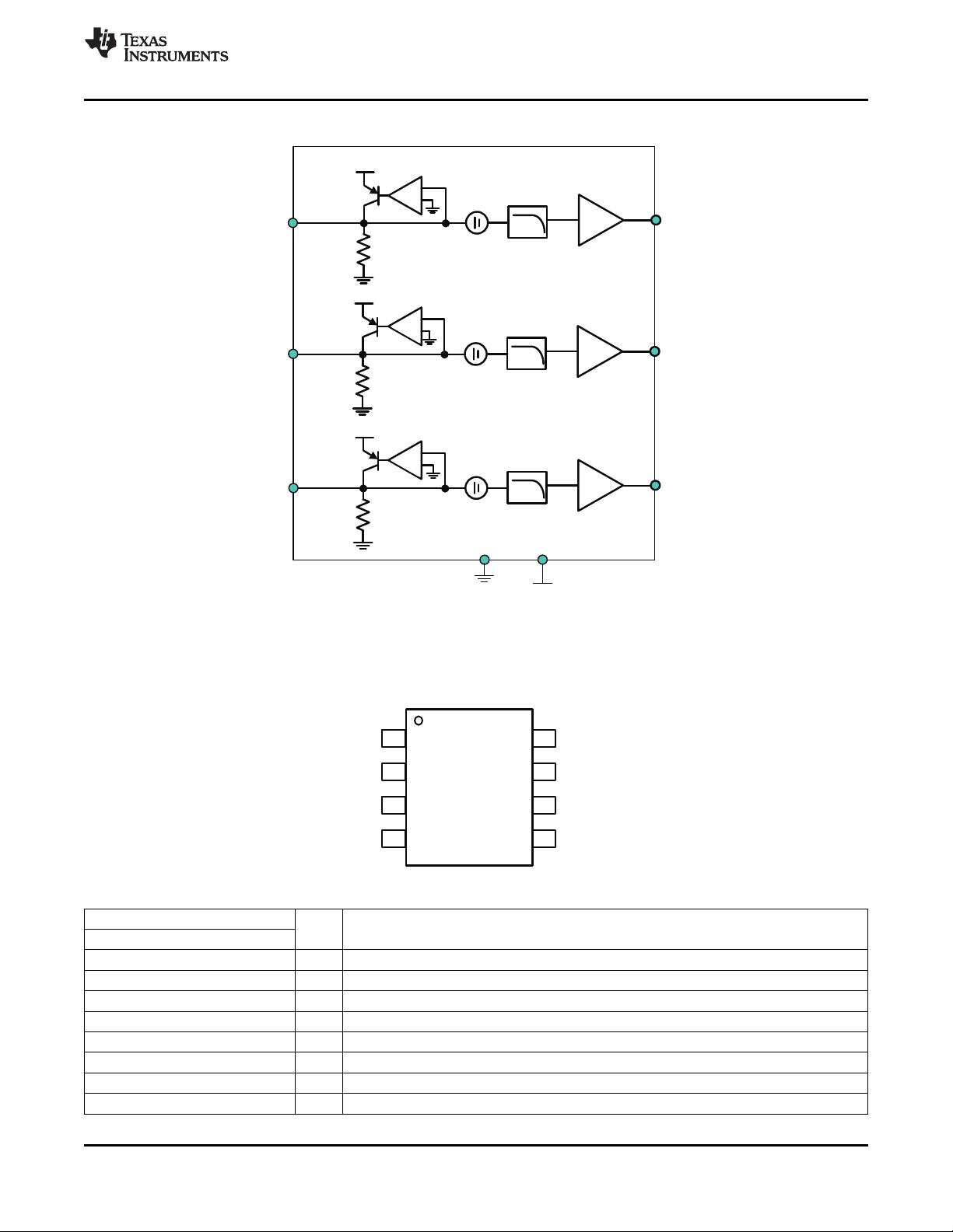
3-Channel SDTV Video Amplifier With 5
th
-Order Filters and 6-dB Gain
Check for Samples: THS7314
1
FEATURES
DESCRIPTION
• 3 SDTV Video Amplifiers for CVBS, S-Video,
Y'P'
B
P'
R
480i/576i, Y'U'V', or G'B'R' (R'G'B')
Fabricated using the Silicon-Germanium (SiGe)
BiCom-III process, the THS7314 is a low power
• Integrated Low-Pass Filters
single-supply 3-V to 5-V 3-channel integrated video
– 5
th
-Order 8.5-MHz (–3dB) Butterworth
buffer. It incorporates a 5th-order Butterworth filter
– –1dB Passband Bandwidth at 7-MHz
which is useful as a DAC reconstruction filter or an
– 47dB Attenuation at 27-MHz ADC anti-aliasing filter. The 8.5-MHz filter is a perfect
choice for SDTV video which includes Composite
• Versatile Input Biasing
(CVBS), S-Video, Y'U'V', G'B'R' (R'G'B'), and Y'P'
B
P'
R
– DC-Coupled With 285-mV Output Shift
480i/576i.
– AC-Coupled with Sync-Tip Clamp
As part of the THS7314 flexibility, the input can be
– Allows AC-Coupled With DC-Biasing
configured for ac or dc coupled inputs. The 285-mV
• Built-in 6dB Gain (2V/V) output level shift to allow for a full sync dynamic
range at the output with 0-V input. The AC coupled
• 3-V to 5-V Single Supply Operation
modes include a transparent sync-tip clamp option for
• Rail-to-Rail Output:
CVBS, Y', and G'B'R' signals with sync. AC-coupled
– Output Swings Within 100-mV From the
biasing for C'/P'
B
/P'
R
channels is achieved by adding
an external resistor to Vs+.
Rails Allowing AC or DC Output Coupling
– Able to Drive up to 2 Video Lines – 75 Ω
The THS7314 is the perfect choice for all output
buffer applications. Its rail-to-rail output stage with
• Low 16-mA at 3.3-V Total Quiscent Current
6-dB gain allows for both ac and dc line driving. The
• Low Differential Gain/Phase of 0.1% / 0.1°
ability to drive 2-lines, or 75-Ω loads, allows for
• SOIC-8 Package
maximum flexibility as a video line driver. The 16-mA
total quiescent current at 3.3-V makes it an excellent
APPLICATIONS
choice for USB powered, portable, or other power
sensitive video applications.
• Set Top Box Output Video Buffering
• PVR/DVDR Output Buffering
The THS7314 is available in a small SOIC-8 package
• USB/Portable Low Power Video Buffering that is RoHS compliant.
Figure 1. 3.3-V Single-Supply DC-Input/DC Output Coupled Video Line Driver
1
Please be aware that an important notice concerning availability, standard warranty, and use in critical applications of Texas
Instruments semiconductor products and disclaimers thereto appears at the end of this data sheet.
PRODUCTION DATA information is current as of publication date.
© 2006–2011, Texas Instruments Incorporated
Products conform to specifications per the terms of the Texas
Instruments standard warranty. Production processing does not
necessarily include testing of all parameters.
THS7314
SLOS513A –DECEMBER 2006– REVISED MARCH 2011
www.ti.com
This integrated circuit can be damaged by ESD. Texas Instruments recommends that all integrated circuits be handled with
appropriate precautions. Failure to observe proper handling and installation procedures can cause damage.
ESD damage can range from subtle performance degradation to complete device failure. Precision integrated circuits may be more
susceptible to damage because very small parametric changes could cause the device not to meet its published specifications.
PACKAGING/ORDERING INFORMATION
PACKAGED DEVICES PACKAGE TYPE
(1)
TRANSPORT MEDIA, QUANTITY
THS7314D Rails, 75
SOIC-8
THS7314DR Tape and Reel, 2500
(1) For the most current package and ordering information, see the Package Option Addendum at the end of this document, or see the TI
website at www.ti.com.
ABSOLUTE MAXIMUM RATINGS
over operating free-air temperature range (unless otherwise noted)
(1)
VALUE UNIT
Supply voltage, V
S+
to GND 5.5 V
V
I
Input voltage –0.4 V to V
S+
I
O
Output current 90 mA
Continuous power dissipation See Dissipation Rating Table
T
J
Maximum junction temperature, any condition
(2)
150 °C
T
J
Maximum junction temperature, continuous operation, long term reliability
(3)
125 °C
T
stg
Storage temperature range –65 to 150 °C
HBM 2000
ESD ratings CDM 1500 V
MM 200
(1) Stresses above those listed under absolute maximum ratings may cause permanent damage to the device. These are stress ratings
only and functional operation of the device at these or any other conditions beyond those indicated under recommended operating
conditions is not implied. Exposure to absolute maximum rated conditions for extended periods may degrade device reliability.
(2) The absolute maximum junction temperature under any condition is limited by the constraints of the silicon process.
(3) The absolute maximum junction temperature for continuous operation is limited by the package constraints. Operation above this
temperature may result in reduced reliability and/or lifetime of the device.
DISSIPATION RATINGS
POWER RATING
(1)
θ
JC
θ
JA
(T
J
= 125°C)
PACKAGE
(°C/W) (°C/W)
T
A
= 25°C T
A
= 85°C
SOIC-8 (D) 50 130
(2)
769 mW 308 mW
(1) Power rating is determined with a junction temperature of 125°C. This is the point where performance starts to degrade and long-term
reliability starts to be reduced. Thermal management of the final PCB should strive to keep the junction temperature at or below 125°C
for best performance and reliability.
(2) This data was taken with the JEDEC High-K test PCB. For the JEDEC low-K test PCB, the θ
JA
is 196°C/W.
RECOMMENDED OPERATING CONDITIONS
MIN MAX UNIT
V
S+
Supply voltage 3 5 V
T
A
Ambient temperature –40 85 °C
2 Submit Documentation Feedback © 2006–2011, Texas Instruments Incorporated
Product Folder Link(s) :THS7314
LPF
6dB
LPF
6dB
LPF
6dB
Channel3
Output
Channel1
Output
Level
Shift
800kW
Channel2
Output
800kW
3Vto5V
800kW
Channel3
Input
Sync-Tip
Clamp
(DCRestore)
5-Pole
8.5-MHz
Channel1
Input
Channel2
Input
Sync-Tip
Clamp
(DCRestore)
Sync-Tip
Clamp
(DCRestore)
5-Pole
8.5-MHz
gm
+
-
5-Pole
8.5-MHz
+Vs
+Vs
+Vs
Level
Shift
Level
Shift
gm
+
-
gm
+
-
5
8
7
6
1
2
3
4
CH.1IN
CH.2IN
CH.3IN
V
S+
CH.1OUT
CH.2OUT
CH.3OUT
GND
THS7314
THS7314
www.ti.com
SLOS513A –DECEMBER 2006– REVISED MARCH 2011
FUNCTIONAL DIAGRAM
PIN CONFIGURATION
SOIC-8 (D)
(TOP VIEW)
PIN FUNCTIONS
PIN
I/O DESCRIPTION
NAME NO. SOIC-8
CH. 1 – INPUT 1 I Video Input – Channel 1
CH. 2 – INPUT 2 I Video Input – Channel 2
CH. 3 – INPUT 3 I Video Input – Channel 3
+Vs 4 I Positive Power Supply Pin – connect to 3 V to 5 V.
GND 5 I Ground Pin for all internal circuitry.
CH. 3 – OUTPUT 6 O Video Output – Channel 3
CH. 2 – OUTPUT 7 O Video Output – Channel 2
CH. 1 – OUTPUT 8 O Video Output – Channel 1
© 2006–2011, Texas Instruments Incorporated Submit Documentation Feedback 3
Product Folder Link(s) :THS7314
THS7314
SLOS513A –DECEMBER 2006– REVISED MARCH 2011
www.ti.com
ELECTRICAL CHARACTERISTICS V
S+
= 3.3 V:
R
L
= 150Ω to GND – Reference Figure 2 and Figure 3 (unless otherwise noted)
TYP OVER TEMPERATURE
PARAMETER TEST CONDITIONS
0°C to –40°C to MIN/
25°C 25°C UNITS
70°C 85°C MAX
AC PERFORMANCE
Small-signal bandwidth (–3dB) V
O
– 0.2 V
PP
(1)
8.5 6.7/10.3 6.6/10.5 6.5/10.6 MHz Min/Max
Large-signal bandwidth (–3dB) V
O
– 2 V
PP
(1)
8.5 6.7/10.3 6.6/10.5 6.5/10.6 MHz Min/Max
–1dB Passband bandwidth 7 MHz Typ
Attenuation f = 6 MHz
(2)
0.45 –0.3/2.4 –0.35/2.5 –0.4/2.6 dB Min/Max
With respect to 100kHz f = 27 MHz
(2)
47 36 35 34 dB Min
Group delay f = 100 kHz 57 ns Typ
Group delay variation
f = 5.1 MHz 10.2 ns Typ
with respect to 100kHz
Channel-to-channel delay 0.3 ns Typ
Differential gain NTSC / PAL 0.1 / 0.1 % Typ
Differential phase NTSC / PAL 0.1 / 0.1 ° Typ
Total harmonic distortion f = 1 MHz; V
O
= 2 V
PP
; AC coupled I/O –66 dB Typ
Signal to noise ratio NTC-7 Weighting, 100kHz to 4.2MHz 79.6 dB Typ
Channel-to-channel crosstalk f = 1 MHz, Worst Case Channels –60 dB Typ
AC Gain – All channels 6 5.7/6.3 5.65/6.35 5.65/6.35 dB Min/Max
Output Impedance f = 5 MHz 0.63 Ω Typ
DC PERFORMANCE
Biased output voltage V
I
= 0 V 285 210/370 200/380 190/390 mV Min/Max
Input voltage range DC input, limited by output –0.1/1.46 V Typ
Sync tip clamp charge current V
I
= –0.1 V 180 μA Typ
Input resistance 800 kΩ Typ
Input capacitance 2 pF Typ
OUTPUT CHARACTERISTICS
R
L
= 150 Ω to Midrail 3.15 V Typ
R
L
= 150 Ω to GND 3.1 2.85 2.75 2.75 V Min
High output voltage swing
R
L
= 75 Ω to Midrail 3.1 V Typ
R
L
= 75 Ω to GND 3 V Typ
R
L
= 150 Ω to Midrail (V
I
= –0.2V) 0.15 V Typ
R
L
= 150 Ω to GND (V
I
= –0.2V) 0.1 0.17 0.2 0.21 V Max
Low output voltage swing
R
L
= 75 Ω to Midrail (V
I
= –0.2V) 0.3 V Typ
R
L
= 75 Ω to GND (V
I
= –0.2V) 0.1 V Typ
Output current (sourcing) R
L
= 10 Ω to Midrail 80 mA Typ
Output current (sinking) R
L
= 10 Ω to Midrail 70 mA Typ
POWER SUPPLY
Maximum operating voltage See
(1)
3.3 5.5 5.5 5.5 V Max
Minimum operating voltage See
(1)
3.3 2.85 2.85 2.85 V Min
Maximum quiescent current V
I
= 0V 16 20 22 24 mA Max
Minimum quiescent current V
I
= 0V 16 12 11.6 11 mA Min
Power Supply Rejection (+PSRR) 52 dB Typ
(1) The Min/Max values listed for this specification are specified by design and characterization only.
(2) 3.3-V Supply Filter specifications are specified by 100% testing at 5-V supply along with design and characterization only.
4 Submit Documentation Feedback © 2006–2011, Texas Instruments Incorporated
Product Folder Link(s) :THS7314
THS7314
www.ti.com
SLOS513A –DECEMBER 2006– REVISED MARCH 2011
ELECTRICAL CHARACTERISTICS V
S+
= 5 V:
R
L
= 150Ω to GND – Reference Figure 2 and Figure 3 (unless otherwise noted)
TYP OVER TEMPERATURE
PARAMETER TEST CONDITIONS
0°C to –40°C to MIN/
25°C 25°C UNITS
70°C 85°C MAX
AC PERFORMANCE
Small-signal bandwidth (–3dB) V
O
– 0.2 V
PP
(1)
8.5 6.7/10.3 6.6/10.5 6.5/10.6 MHz Min/Max
Large-signal bandwidth (–3dB) V
O
– 2 V
PP
(1)
8.5 6.7/10.3 6.6/10.5 6.5/10.6 MHz Min/Max
–1dB Passband bandwidth 7 MHz Typ
Attenuation f = 6 MHz 0.45 –0.3/2.4 –0.35/2.5 –0.4/2.6 dB Min/Max
With respect to 100kHz f = 27 MHz 47 36 35 34 dB Min
Group delay f = 100 kHz 57 ns Typ
Group delay variation
f = 5.1 MHz 10 ns Typ
with respect to 100kHz
Channel-to-channel delay 0.3 ns Typ
Differential gain NTSC / PAL 0.1 / 0.1 % Typ
Differential phase NTSC / PAL 0.1 / 0.1 ° Typ
Total harmonic distortion f = 1 MHz; V
O
=2 V
PP
–66 dB Typ
Signal to noise ratio NTC-7 Weighting, 100kHz to 4.2MHz 79.6 dB Typ
Channel-to-channel crosstalk f = 1 MHz, Worst Case Channels –60 dB Typ
AC Gain – All channels 6 5.7/6.3 5.65/6.35 5.65/6.35 dB Min/Max
Output Impedance f = 5 MHz 0.62 Ω Typ
DC PERFORMANCE
Biased output voltage V
I
= 0 V 290 210/370 200/380 190/390 mV Min/Max
Input voltage range Limited by output –0.1/2.3 V Typ
Sync tip clamp charge current V
I
= –0.1V 180 μA Typ
Input resistance 800 kΩ Typ
Input capacitance 2 pF Typ
OUTPUT CHARACTERISTICS
R
L
= 150 Ω to Midrail 4.85 V Typ
R
L
= 150 Ω to GND 4.7 4.2 4.1 4.1 V Min
High output voltage swing
R
L
= 75 Ω to Midrail 4.7 V Typ
R
L
= 75 Ω to GND 4.5 V Typ
R
L
= 150 Ω to Midrail (V
I
= –0.2V) 0.2 V Typ
R
L
= 150 Ω to GND (V
I
= –0.2V) 0.12 0.23 0.26 0.27 V Max
Low output voltage swing
R
L
= 75 Ω to Midrail (V
I
= –0.2V) 0.35 V Typ
R
L
= 75 Ω to GND (V
I
= –0.2V) 0.1 V Typ
Output current (sourcing) R
L
= 10 Ω to Midrail 90 mA Typ
Output current (sinking) R
L
= 10 Ω to Midrail 85 mA Typ
POWER SUPPLY
Maximum operating voltage See
(1)
5 5.5 5.5 5.5 V Max
Minimum operating voltage See
(1)
5 2.85 2.85 2.85 V Min
Maximum quiescent current V
I
= 0V 17 22 24 25 mA Max
Minimum quiescent current V
I
= 0V 17 12.5 12 11.5 mA Min
Power Supply Rejection (+PSRR) 55 dB Typ
(1) The Min/Max values listed for this specification are specified by design and characterization only.
© 2006–2011, Texas Instruments Incorporated Submit Documentation Feedback 5
Product Folder Link(s) :THS7314
剩余31页未读,继续阅读
资源评论
不觉明了
- 粉丝: 3164
- 资源: 5429
上传资源 快速赚钱
- 我的内容管理 展开
- 我的资源 快来上传第一个资源
- 我的收益 登录查看自己的收益
- 我的积分 登录查看自己的积分
- 我的C币 登录后查看C币余额
- 我的收藏
- 我的下载
- 下载帮助
安全验证
文档复制为VIP权益,开通VIP直接复制
信息提交成功