TI-THS4521-HT.pdf
需积分: 11 129 浏览量
2022-11-24
23:42:34
上传
评论 5
收藏 1.03MB PDF 举报

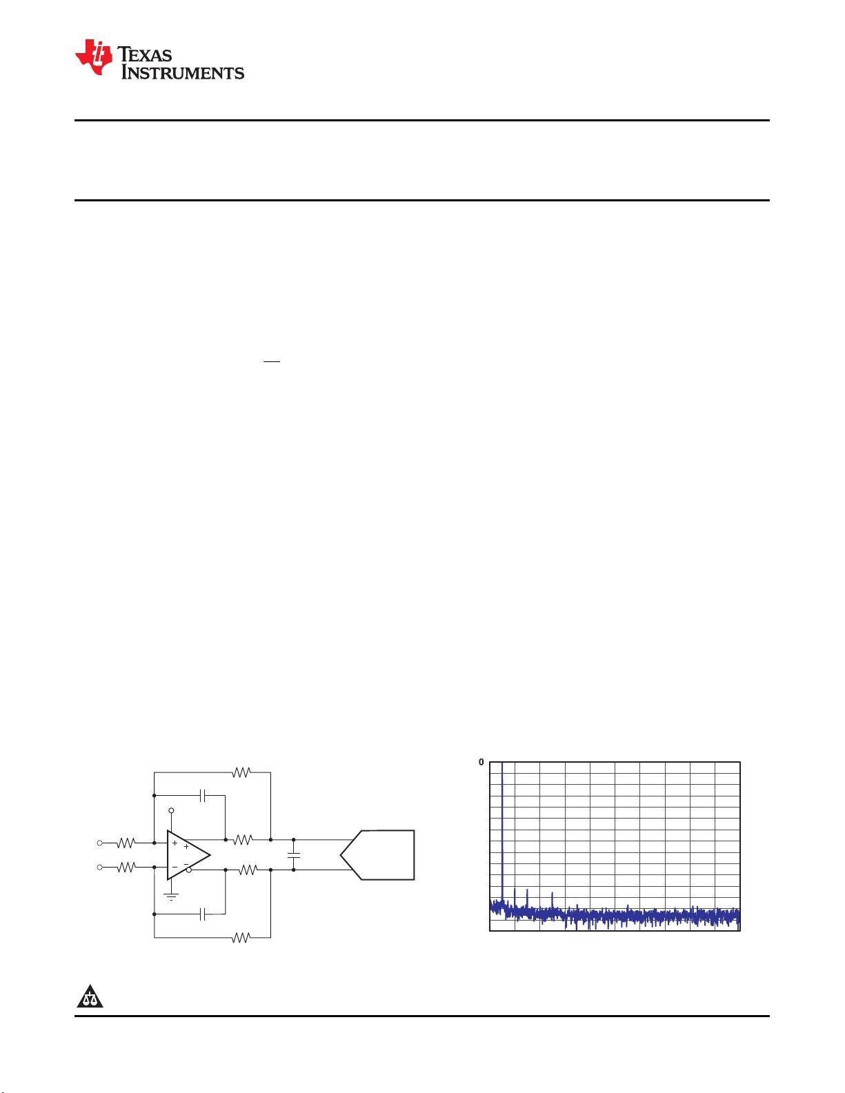
-150
-140
-130
-120
-110
-100
-90
-80
-70
-60
-50
-40
-30
-20
-10
0 2k 4k 6k 8k 10k 12k 14k 16k 18k 20k
Frequency (Hz)
Magnitude (dBV)
THS4521 ADS1278 (CH 1)
49.9 W
1 kW
49.9 W
V
IN+
V
IN-
3.3 V
1 kW
1 kW
2.2 nF
AINP1
AINN1
1.5 nF
1.5 nF
1 kW
THS4521-HT
www.ti.com.cn
ZHCS261D –APRIL 2011–REVISED MAY 2012
极极低低功功率率,,负负电电源源轨轨输输入入,,
轨轨到到轨轨输输出出,,完完全全差差分分放放大大器器
查查询询样样品品: THS4521-HT
1
特特性性
• 全全差差分分架架构构 应应用用范范围围
• 带带宽宽:: 40.7 MHz (210°C)
• 潜潜孔孔钻钻进进
• 转转换换速速率率:: 353.5 V/μs (210°C)
• 高高温温环环境境
• HD
2
: –96 dBc,,在在 1 kHz
支支持持极极端端温温度度应应用用
(1 V
RMS
, R
L
= 1 kΩ) (210°C)
• HD
3
: –91.5 dBc,,在在 1 kHz
• 受受控控基基线线
(1 V
RMS
, R
L
= 1 kΩ) (210°C)
• 一一个个组组装装/测测试试场场所所
• 输输入入电电压压噪噪声声:: 19.95 nV/√Hz (f = 100 kHz)
• 一一个个制制造造场场所所
• 开开环环增增益益:: 90 dB ((典典型型值值))(210°C)
• 可可在在极极端端温温度度范范围围 (–55°C/210°C)
• NRI—负负轨轨输输入入
下下工工作作
(1)
• RRO—轨轨至至轨轨输输出出
• 产产品品生生命命周周期期有有所所延延长长
• 输输出出共共模模控控制制 ((具具有有低低失失调调及及低低漂漂移移))
• 拓拓展展的的产产品品变变更更通通知知
• 电电源源
• 产产品品可可追追溯溯性性
– 电电压压:: 2.5 V (±1.25 V) 至至 3.3 V (±1.65 V)
• 德德州州仪仪器器的的高高温温产产品品运运用用了了高高度度优优化化的的硅硅片片((芯芯
片片))解解决决方方案案,,此此类类解解决决方方案案在在设设计计与与工工艺艺方方面面均均
– 电电流流::每每通通道道 1.4 mA ((在在 3.3 V 电电压压下下))
有有所所强强化化,,以以在在扩扩展展的的温温度度范范围围内内实实现现性性能能的的最最大大
• 断断电电能能力力:: 10 µA ((典典型型值值))(210°C)
化化。。
(1) 可定制工作温度范围
说说明明
THS4521 是一款极低功率,完全差分运算放大器,此放大器具有轨到轨输出和一个包括负电源轨在内的输入共模
范围。 这个放大器设计用于低功率数据采集系统和高密度应用,在此类应用中功率耗散是一个关键参数,此放大器
还在音频应用中提供出色的性能。
THS4521 具有准确的输出共模控制能力,可在驱动模数转换器 (ADC) 时实现 DC 耦合。 这种控制能力与一个低于
负电源轨的输入共模范围以及轨至轨输出相结合,可在单端接地参考信号源之间实现简易型连接。 此外,该器件还
非常适合只采用单 2.5-V 至 3.3-V 电源和地面电源来驱动逐次逼近寄存器型 (SAR) 和增量-累加型 (ΔΣ) ADC。
THS4521 针对 –55°C 至 210°C 的工作温度范围进行了特性分析。
1
Please be aware that an important notice concerning availability, standard warranty, and use in critical applications of
Texas Instruments semiconductor products and disclaimers thereto appears at the end of this data sheet.
PRODUCTION DATA information is current as of publication date.
Copyright © 2011–2012, Texas Instruments Incorporated
Products conform to specifications per the terms of the Texas
Instruments standard warranty. Production processing does not English Data Sheet: SBOS548
necessarily include testing of all parameters.
剩余27页未读,继续阅读
资源评论


