没有合适的资源?快使用搜索试试~ 我知道了~
TI-THS4541.pdf
需积分: 9 0 下载量 116 浏览量
2022-11-24
23:41:37
上传
评论 5
收藏 2.39MB PDF 举报
温馨提示
试读
64页
TI-THS4541.pdf
资源推荐
资源详情
资源评论
C2
100 nF
Rf1
402
Rload
500
Rg1
191
C1
100 nF
Rg2
221
Rt
60.2
Output
Measurement
Point
THS4541 Wideband,
Fully-Differential Amplifier
50-Input Match Gain of
2 V/V from Rt Single-Ended
Source to Differential Output
Vocm
Rf2
402
50-
Source
+
±
Vcc
+
±
Vocm
Vcc
FDA
PD
Frequency (MHz)
Distortion (dBc)
0.1 1 10 50
-140
-130
-120
-110
-100
-90
-80
-70
-60
-50
D013
HD2
HD3
Product
Folder
Sample &
Buy
Technical
Documents
Tools &
Software
Support &
Community
THS4541
SLOS375 –AUGUST 2014
THS4541 Negative Rail Input, Rail-to-Rail Output, Precision, 850-MHz
Fully Differential Amplifier
1 Features 3 Description
The THS4541 is a low-power, voltage-feedback, fully
1
• Fully Differential Amplifier (FDA) Architecture
differential amplifier (FDA) with an input common-
• Bandwidth: 500 MHz (G = 2 V/V)
mode range below the negative rail, and rail-to-rail
• Gain Bandwidth Product: 850 MHz
output. Designed for low-power data acquisition
systems where high density is critical in a high-
• Slew Rate: 1500 V/µs
performance analog-to-digital converter (ADC) or
• HD
2
: –95 dBc at 10 MHz (2 V
PP
, R
L
= 500 Ω)
digital-to-analog converter (DAC) interface design.
• HD
3
: –90 dBc at 10 MHz (2 V
PP
, R
L
= 500 Ω)
The THS4541 features the negative-rail input
• Input Voltage Noise: 2.2 nV/Hz (f > 100 kHz)
required when interfacing a dc-coupled, ground-
• Low offset drift: ±0.5 µV/°C (typ)
centered, source signal. This negative-rail input, with
rail-to-rail output, allows for easy interface between
• Negative Rail Input (NRI)
single-ended, ground-referenced, bipolar signal
• Rail-to-Rail Output (RRO)
sources and a wide variety of SAR, ΔΣ, or pipeline
• Robust Operation for Rload ≥ 50 Ω
ADCs using only a single +2.7-V to +5.4-V power
• Output Common-Mode Control
supply.
• Power Supply:
The THS4541 is characterized for operation over the
– Single-Supply Voltage Range: 2.7 V to 5.4 V wide temperature range of –40°C to 125 ° C available
in 16-pin VQFN and 10-pin WQFN packages.
– Split-Supply Voltage Range: ±1.35 V to ±2.7 V
– Quiescent Current: 10.1 mA (5-V Supply)
Device Information
(1)
• Power-Down Capability: 2 µA (typ)
PART NUMBER PACKAGE BODY SIZE (NOM)
VQFN (16) 3.00 mm × 3.00 mm
THS4541
2 Applications
WQFN (10) 2.00 mm × 2.00 mm
• Low-Power, High-Performance ADC Driver
(1) For all available packages, see the package option addendum
at the end of the datasheet.
– SAR, ΔΣ, and Pipeline
• Low Power, High Performance
(DC or AC Coupled)
– Single-Ended to Differential Amplifier
– Differential to Differential Amplifier
• Differential Active Filters
• Differential Transimpedance for DAC Outputs
• DC- or AC-Coupled Interface to the ADC3xxx
Family of Low-Power, High-Performance ADCs
• Pin-Compatible Upgrade to ADA4932-1 (RGT)
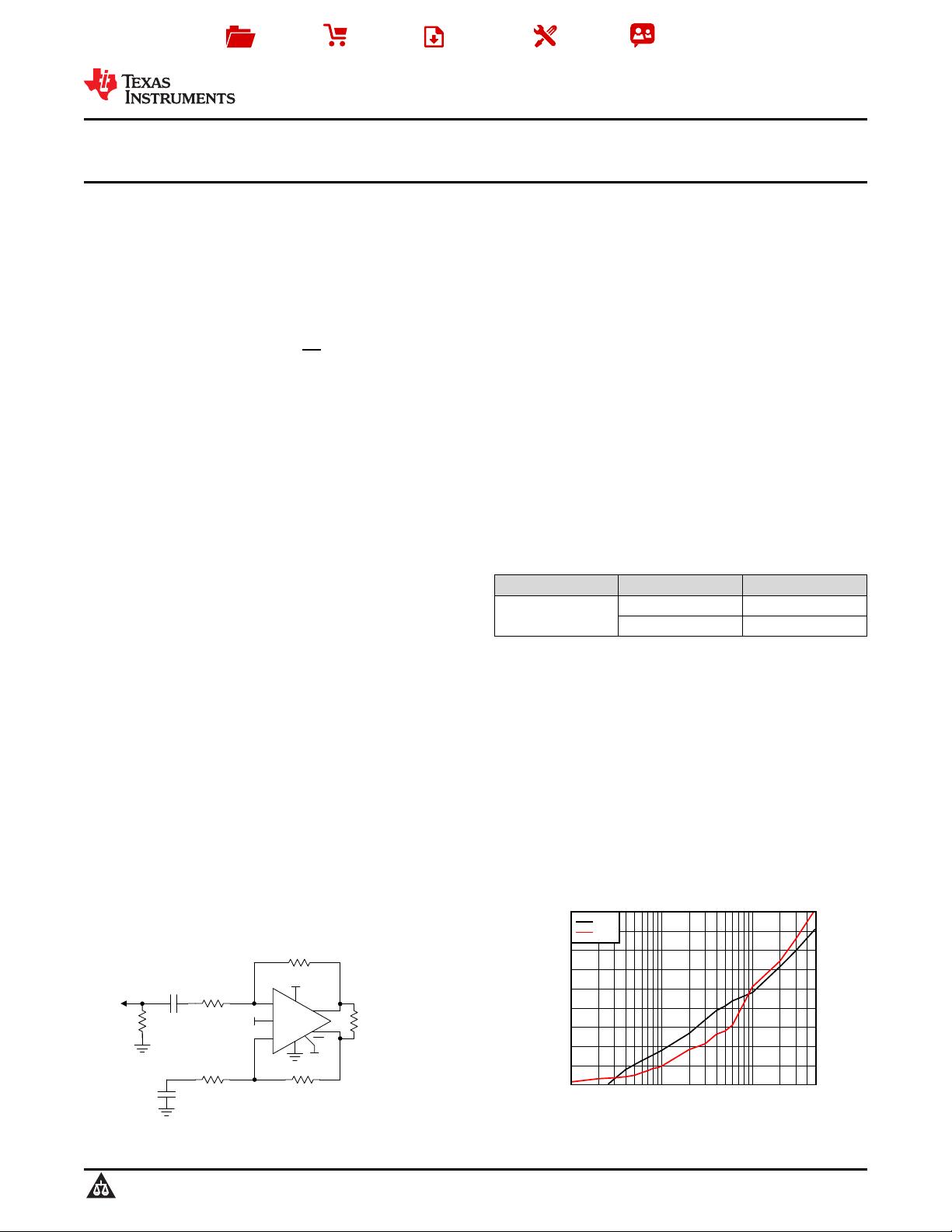
Simplified Schematic Single to Differential Gain of 2, 2-V
PP
Output
1
An IMPORTANT NOTICE at the end of this data sheet addresses availability, warranty, changes, use in safety-critical applications,
intellectual property matters and other important disclaimers. PRODUCTION DATA.
THS4541
SLOS375 –AUGUST 2014
www.ti.com
Table of Contents
8.6 Factors Influencing Harmonic Distortion................. 31
1 Features.................................................................. 1
8.7 Driving Capacitive Loads ........................................ 32
2 Applications ........................................................... 1
8.8 Thermal Analysis..................................................... 32
3 Description ............................................................. 1
9 Detailed Description............................................ 33
4 Revision History..................................................... 2
9.1 Overview ................................................................. 33
5 Device Family Comparison................................... 3
9.2 Functional Block Diagram ....................................... 34
6 Pin Configuration and Functions......................... 3
9.3 Feature Description................................................. 35
7 Specifications......................................................... 4
9.4 Device Functional Modes........................................ 36
7.1 Absolute Maximum Ratings ...................................... 4
10 Application And Implementation....................... 44
7.2 Handling Ratings....................................................... 4
10.1 Application Information.......................................... 44
7.3 Recommended Operating Conditions....................... 4
10.2 Typical Applications .............................................. 44
7.4 Thermal Information.................................................. 4
11 Power-Supply Recommendations ..................... 49
7.5 Electrical Characteristics: Vs+ – Vs– = 5 V ............. 5
12 Layout................................................................... 50
7.6 Electrical Characteristics: Vs+ – Vs– = 3 V ............. 8
12.1 Layout Guidelines ................................................. 50
7.7 Typical Characteristics: 5-V Single Supply ............. 11
12.2 Layout Example .................................................... 51
7.8 Typical Characteristics: 3-V Single Supply ............. 14
13 Device and Documentation Support ................. 52
7.9 Typical Characteristics: 3-V to 5-V Supply Range.. 17
13.1 Device Support...................................................... 52
8 Parameter Measurement Information ................ 21
13.2 Trademarks........................................................... 52
8.1 Example Characterization Circuits.......................... 21
13.3 Electrostatic Discharge Caution............................ 52
8.2 Frequency-Response Shape Factors ..................... 23
13.4 Glossary................................................................ 52
8.3 I/O Headroom Considerations ................................ 26
14 Mechanical, Packaging, and Orderable
8.4 Output DC Error and Drift Calculations and the Effect
Information ........................................................... 52
of Resistor Imbalances ............................................ 28
8.5 Noise Analysis......................................................... 30
4 Revision History
DATE REVISION NOTES
August 2014 * Initial release.
2 Submit Documentation Feedback Copyright © 2014, Texas Instruments Incorporated
Product Folder Links: THS4541
1315 1416
86 75
FB–
FB+
IN+
IN–
PD
OUT–
OUT+
Vocm
Vs–
Vs+
Vs–
Vs–
Vs–
Vs+
Vs+
Vs+
1
3
2
4
9
10
11
12
10
1
3
2
4
6
7
8
9
IN–
PD
OUT–
OUT+
Vocm
Vs–
Vs+
IN+
NC
NC
5
THS4541
www.ti.com
SLOS375 –AUGUST 2014
5 Device Family Comparison
INPUT NOISE
DEVICE BW (MHz) I
Q
(mA) THD (dBc) 2 V
PP
AT 100 kHz (nV/√Hz) RAIL-TO-RAIL
THS4531A 36 0.25 –104 10 Out
THS4521 145 0.95 –102 4.6 Out
THS4520 620 14.2 –107 2.0 Out
6 Pin Configuration and Functions
RGT Package
RUN Package
VQFN-16
WQFN-10
(Top View)
(Top View)
Pin Functions
PIN
NO.
NAME
RGT
(1)
RUN I/O DESCRIPTION
FB+ 4 — O Noninverted (positive) output feedback
FB– 1 — O Inverted (negative) output feedback
IN+ 2 4 I Noninverting (positive) amplifier input
IN– 3 6 I Inverting (negative) amplifier input
NC — 2, 8 — No internal connection
OUT+ 10 9 O Noninverted (positive) amplifier output
OUT– 11 1 O Inverted (negative) amplifier output
PD 12 3 I Power down. PD = logic low = power off mode; PD = logic high = normal operation.
Vocm 9 7 I Common-mode voltage input
Vs+ 5, 6, 7, 8 10 I Positive power-supply input
13, 14, 15,
Vs– 5 I Negative power-supply input
16
(1) Solder the exposed thermal pad (RGT package) to a heat-spreading power or ground plane. This pad is electrically isolated from the
die.
Copyright © 2014, Texas Instruments Incorporated Submit Documentation Feedback 3
Product Folder Links: THS4541
THS4541
SLOS375 –AUGUST 2014
www.ti.com
7 Specifications
7.1 Absolute Maximum Ratings
over operating free-air temperature range (unless otherwise noted)
(1)
MIN MAX UNIT
Supply voltage, Vs+ – Vs– 5.5 V
Voltage Input/output voltage range (Vs–) – 0.5 (Vs+) + 0.5 V
Differential input voltage ±1 V
Continuous input current ±20 mA
Current Continuous output current ±80 mA
Continuous power dissipation See Thermal Information table and Thermal Analysis section
Maximum junction temperature 150 °C
Temperature
Operating free-air temperature range –40 125 °C
(1) Stresses beyond those listed under Absolute Maximum Ratings may cause permanent damage to the device. These are stress ratings
only, which do not imply functional operation of the device at these or any other conditions beyond those indicated under Recommended
Operating Conditions. Exposure to absolute-maximum-rated conditions for extended periods may affect device reliability.
7.2 Handling Ratings
MIN MAX UNIT
T
stg
Storage temperature range –65 150 °C
Human body model (HBM), per ANSI/ESDA/JEDEC JS-001, all pins
(1)
–2000 2000
Electrostatic
V
(ESD)
Charged device model (CDM), per JEDEC specification JESD22-C101, all pins
(2)
–500 500 V
discharge
Machine model
(2)
–150 150
(1) JEDEC document JEP155 states that 500-V HBM allows safe manufacturing with a standard ESD control process.
(2) JEDEC document JEP157 states that 250-V CDM allows safe manufacturing with a standard ESD control process.
7.3 Recommended Operating Conditions
over operating free-air temperature range (unless otherwise noted)
MIN NOM MAX UNIT
Vs+ Single-supply voltage 2.7 5 5.4 V
T
A
Ambient temperature –40 25 125 °C
7.4 Thermal Information
THS4541
THERMAL METRIC
(1)
RGT (VQFN) RUN (WQFN) UNIT
16 PINS 10 PINS
R
θJA
Junction-to-ambient thermal resistance 52 146
R
θJC(top)
Junction-to-case (top) thermal resistance 69 75
R
θJB
Junction-to-board thermal resistance 25 39
°C/W
ψ
JT
Junction-to-top characterization parameter 2.7 14
ψ
JB
Junction-to-board characterization parameter 25 105
R
θJC(bot)
Junction-to-case (bottom) thermal resistance 9.3 47
(1) For more information about traditional and new thermal metrics, see the IC Package Thermal Metrics application report, SPRA953.
4 Submit Documentation Feedback Copyright © 2014, Texas Instruments Incorporated
Product Folder Links: THS4541
THS4541
www.ti.com
SLOS375 –AUGUST 2014
7.5 Electrical Characteristics: Vs+ – Vs– = 5 V
At T
A
≈ 25°C, Vocm = open (defaults midsupply), V
OUT
= 2 V
PP
, Rf = 402 Ω, Rload = 499 Ω, 50-Ω input match, G = 2 V/V,
single-ended input, differential output, and PD = +Vs, unless otherwise noted. See Figure 61 for an ac-coupled gain of a
2-V/V test circuit, and Figure 63 for a dc-coupled gain of a 2-V/V test circuit.
TEST
PARAMETER TEST CONDITIONS MIN TYP MAX UNIT LEVEL
(1)
AC PERFORMANCE
Vout = 100 mV
PP
, G = 1 620 MHz C
Vout = 100 mV
PP
, G = 2 (see Figure 61) 500 MHz C
Small-signal bandwidth
Vout = 100 mV
PP
, G = 5 210 MHz C
Vout = 100 mV
PP
, G = 10 125 MHz C
Gain-bandwidth product Vout = 100 mV
PP
, G = 20 850 MHz C
Large-signal bandwidth Vout = 2 V
PP
, G = 2 (see Figure 61) 340 MHz C
Bandwidth for 0.1-dB flatness Vout = 2 V
PP
, G = 2 (see Figure 61) 100 MHz C
Slew rate
(2)
Vout = 2-V
PP
, FPBW (see Figure 61) 1500 V/µs C
Vout = 2-V step, G = 2 input ≤ 0.3 ns t
r
Rise/fall time 1.4 ns C
(see Figure 63)
To 1%, Vout = 2-V step, t
r
= 2 ns, G = 2
4 ns C
(seeFigure 63)
Settling time
To 0.1%,Vout = 2-V step, t
r
= 2 ns, G = 2
8 ns C
(see Figure 63)
Vout = 2-V step G = 2, input ≤ 0.3 ns t
r
Overshoot and undershoot 10% C
(see Figure 63)
Vout = 2 V
PP
, G = 2, HD2 (see Figure 61) –140 dBc C
100-kHz harmonic distortion
Vout = 2 V
PP
, G = 2, HD3 (see Figure 61) –140 dBc C
Vout = 2 V
PP
, G = 2, HD2 (see Figure 61) –95 dBc C
10-MHz harmonic distortion
Vout = 2 V
PP
, G = 2, HD3 (see Figure 61) –90 dBc C
f = 10 MHz, 100-kHz tone spacing,
2nd-order intermodulation distortion –90 dBc C
Vout envelope = 2 V
PP
(1 V
PP
per tone)
(see Figure 61)
f = 10 MHz, 100-kHz tone spacing,
3rd-order intermodulation distortion –85 dBc C
Vout envelope = 2 V
PP
(1 V
PP
per tone)
(see Figure 61)
Input voltage noise f > 100 kHz 2.2 nV/√Hz C
Input current noise f > 1 MHz 1.9 pA/√Hz C
Overdrive recovery time 2X output overdrive, either polarity 20 ns C
Closed-loop output impedance f = 10 MHz (differential) 0.1 Ω C
(1) Test levels (all values set by characterization and simulation): (A) 100% tested at 25°C; over temperature limits by characterization and
simulation. (B) Not tested in production; limits set by characterization and simulation. (C) Typical value only for information.
(2) This slew rate is the average of the rising and falling time extracted from the large-signal bandwidth as: (V
P
/ √2) · 2π · f
–3dB
.
Copyright © 2014, Texas Instruments Incorporated Submit Documentation Feedback 5
Product Folder Links: THS4541
剩余63页未读,继续阅读
资源评论
不觉明了
- 粉丝: 3164
- 资源: 5429
上传资源 快速赚钱
- 我的内容管理 展开
- 我的资源 快来上传第一个资源
- 我的收益 登录查看自己的收益
- 我的积分 登录查看自己的积分
- 我的C币 登录后查看C币余额
- 我的收藏
- 我的下载
- 下载帮助
最新资源
- Pytorch-pytorch深度学习教程之逻辑回归.zip
- Pytorch-pytorch深度学习教程之双向循环网络.zip
- Pytorch-pytorch深度学习教程之卷积神经网络.zip
- Pytorch-pytorch深度学习教程之前馈神经网络.zip
- Pytorch-pytorch深度学习教程之线性回归.zip
- Pytorch-pytorch深度学习教程之基本操作.zip
- 基于QT的地图可视化桌面系统后台数据库为MySQL5.7源码.zip
- 基于simulink的PLL锁相环系统仿真【包括模型,文档,参考文献,操作步骤】
- 基于EM-GMM模型的目标跟踪和异常行为检测matlab仿真【包括程序,注释,参考文献,操作步骤,说明文档】
- 2109010044_胡晨燕_选课管理数据库设计与实现.prj
资源上传下载、课程学习等过程中有任何疑问或建议,欢迎提出宝贵意见哦~我们会及时处理!
点击此处反馈
安全验证
文档复制为VIP权益,开通VIP直接复制
信息提交成功