TI-TLV9034-Q1.pdf
需积分: 10 10 浏览量
2022-11-22
23:46:05
上传
评论 5
收藏 2.26MB PDF 举报

TLV902x-Q1 and TLV903x-Q1 High-Precision Dual and Quad Automotive Comparators
1 Features
• Qualified for automotive applications
• AEC-Q100 qualified with the following results:
– Device temperature grade 1: –40°C to 125°C
ambient operating temperature range
– Device HBM ESD classification level 2
– Device CDM ESD classification level C6
• 1.65 V to 5.5 V supply range
• Power-On Reset (POR) for known start-up
• Precision input offset voltage 300 μV
• 100ns Typ propagation delay
• Low quiescent current 16 μA per channel
• Rail-to-Rail input voltage range exceeds the rails
• Open-drain output option (TLV902x-Q1)
• Push-pull output option (TLV903x-Q1)
• 2 kV ESD Protection
2 Applications
• Automotive
– HEV/EV and power train
– Infotainment and cluster
– Body control module
• Industrial
3 Description
The TLV902x-Q1 and TLV903x-Q1 are a family
of Automotive grade dual and quad channel
comparators. The family offers low input offset
voltage, integrated Power-On Reset (POR) circuitry,
and fault-tolerant inputs with an excellent speed-to-
power combination with a propagation delay of 100
ns. Operating voltage range of 1.65 V to 5.5 V with a
quiescent supply current of 18 μA per channel.
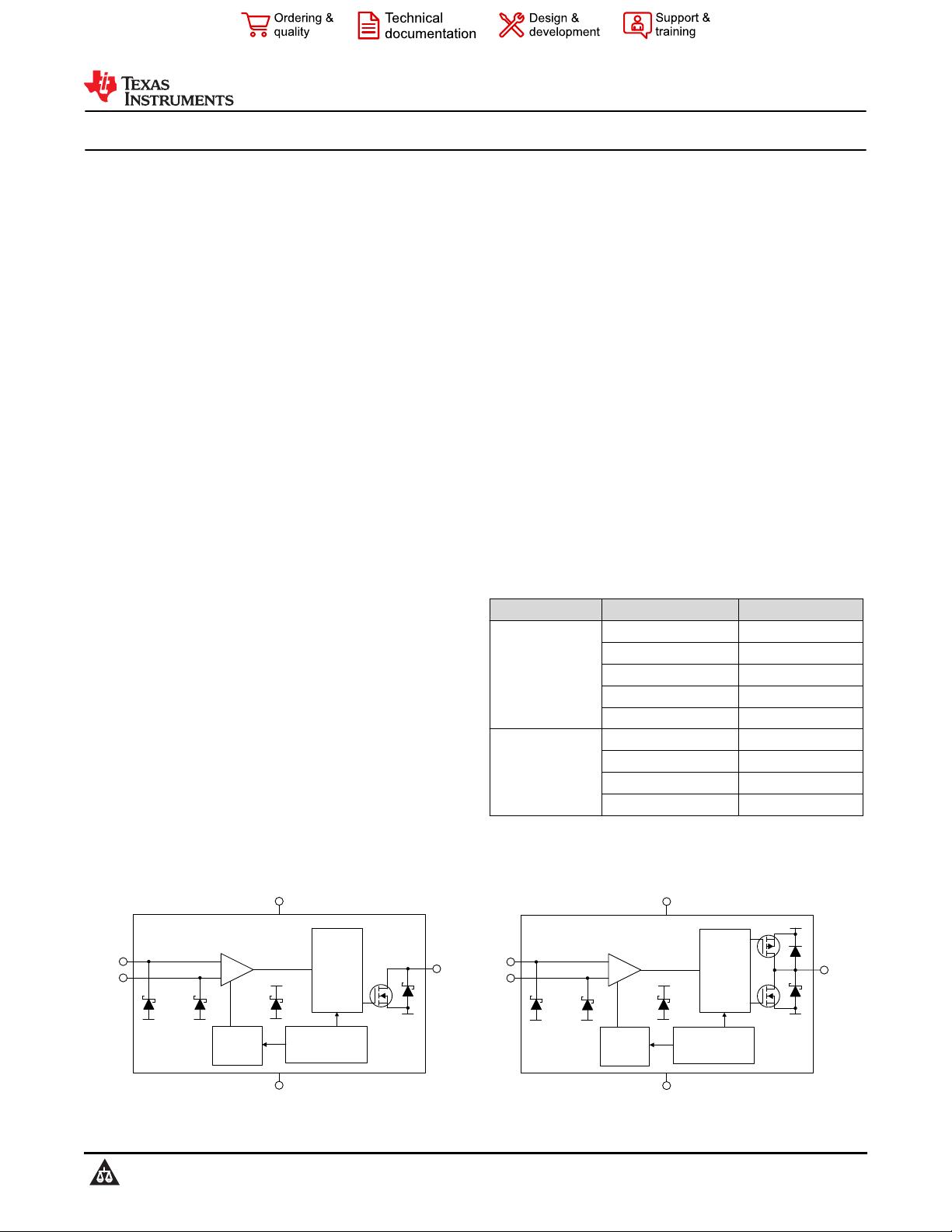
This device family also includes a Power-on Reset
(POR) feature that ensures the output is in a known
state until the minimum supply voltage has been
reached and a small time period passed before the
output starts responding to the inputs. This prevents
output transients during system power-up and power-
down.
These comparators also feature no output phase
inversion with fault-tolerant inputs that can go up
to 6-V without damage. This makes this family
of comparators well suited for precision voltage
monitoring in harsh, noisy environments.
The TLV902x-Q1 comparators have an open-drain
output stage that can be pulled below or beyond the
supply voltage, making it appropriate for low voltage
logic and level translators.
The TLV903x-Q1 comparators have a push-pull
output stage capable of sinking and sourcing
milliamps of current when controlling an LED or
driving a capacitive load such as a MOSFET gate.
The TLV902x-Q1 and TLV903x-Q1 are specified for
the Automotive temperature range of -40°C to +125°C
and are available in a standard leaded and leadless
packages.
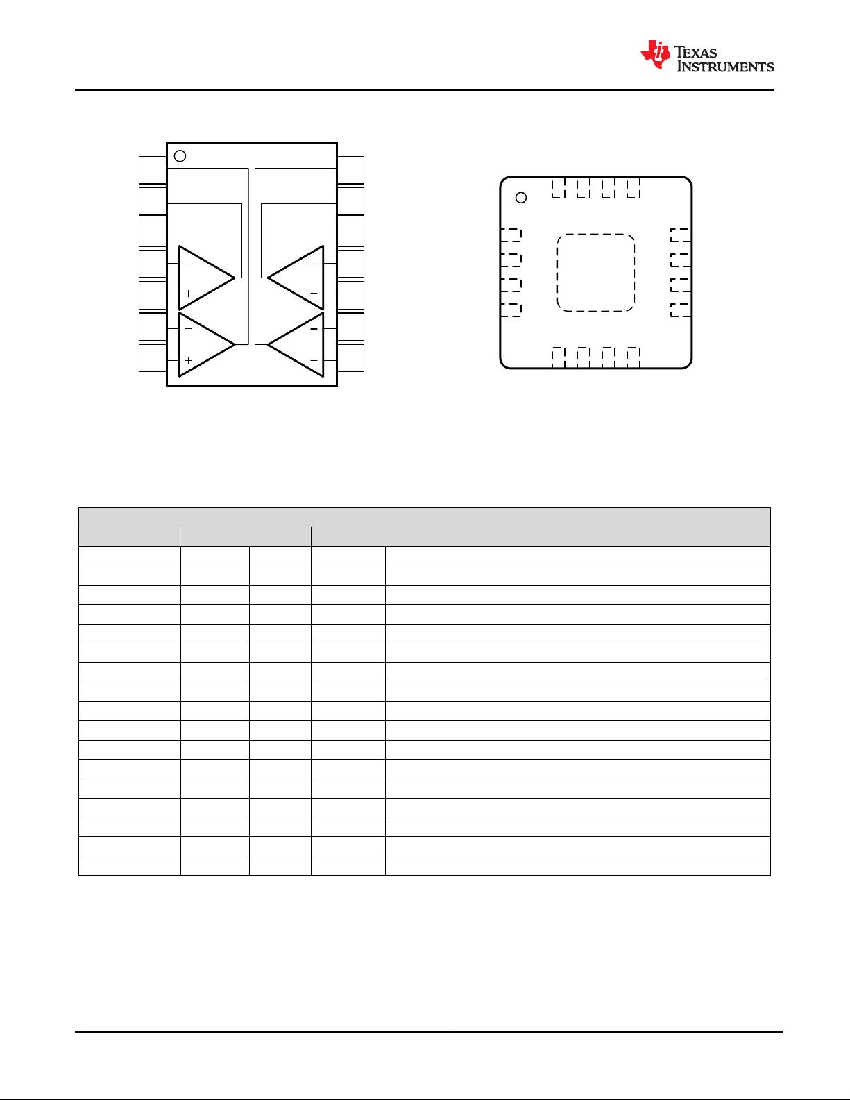
Device Information
PART NUMBER PACKAGE
(1)
BODY SIZE (NOM)
TLV9022-Q1,
TLV9032-Q1
(Dual)
SOIC (8) 3.91 mm × 4.90 mm
TSSOP (8) 3.00 mm × 4.40 mm
VSSOP (8) (Preview) 3.00 mm × 3.00 mm
WSON (8) 2.00 mm × 2.00 mm
SOT-23-THN (8) 1.60 mm × 2.90 mm
TLV9024-Q1,
TLV9034-Q1
(Quad)
SOIC (14) (Preview) 3.91 mm × 8.65 mm
TSSOP (14) 4.40 mm × 5.00 mm
SOT-23 (14) (Preview) 4.20 mm x 2.00 mm
WQFN (16) (Preview) 3.00 mm × 3.00 mm
(1) For all available packages, see the orderable addendum at
the end of the data sheet.
OUT
+
-
IN+
IN-
Bias
Power-On-Reset
(POR)
V+
V-
SNAPBACK
ESD
CLAMPS
V- V-
V-
Output
Control
V-
V+
TLV9022-Q1 and TLV9024-Q1 Block Diagram
OUT
+
-
IN+
IN-
Bias
Power-On-Reset
(POR)
V+
V-
V+
SNAPBACK
ESD
CLAMPS
V-
V-
V-
Output
Control
V-
V+
TLV9032-Q1 and TLV9034-Q1 Block Diagram
TLV9022-Q1, TLV9032-Q1, TLV9024-Q1, TLV9034-Q1
SNOSDA9B – JUNE 2020 – REVISED AUGUST 2021
An IMPORTANT NOTICE at the end of this data sheet addresses availability, warranty, changes, use in safety-critical applications,
intellectual property matters and other important disclaimers. UNLESS OTHERWISE NOTED, this document contains PRODUCTION
DATA.


剩余42页未读,继续阅读


评论0
最新资源