没有合适的资源?快使用搜索试试~ 我知道了~
TI-TLV710-Q1.pdf
需积分: 9 0 下载量 38 浏览量
2022-10-28
23:48:38
上传
评论 5
收藏 2.11MB PDF 举报
温馨提示
试读
27页
TI-TLV710-Q1.pdf
资源详情
资源评论
IN
EN1
EN2
GND
OUT1
OUT2
ON
OFF
ON
OFF
V
IN
C
IN
C
1 F
Ceramic
m
OUT1
C
OUT2
1 F
Ceramic
m
V
OUT1
V
OUT2
OUT1
OUT2
GND
6
5
4
EN1
IN
EN2
1
2
3
TLV7103318-Q1
TLV7101828-Q1
1,5-mm 1,5-mm SON-6
(TOP VIEW)
´
TLV7103318-Q1
TLV7101828-Q1
www.ti.com
SBVS202A –MARCH 2013–REVISED MARCH 2013
Dual, 200-mA, Low-I
Q
Low-Dropout Regulator for Portable Devices
Check for Samples: TLV7103318-Q1 , TLV7101828-Q1
1
FEATURES
APPLICATIONS
• Qualified for Automotive Applications • Automotive Applications
• AEC-Q100 Qualified With the Following • Wireless Handsets, Smart Phones, PDAs
Results:
• MP3 Players and Other Handheld Products
– Device Temperature Grade 1: –40°C to DESCRIPTION
125°C Ambient Operating Temperature
The TLV7103318-Q1 and TLV7101828-Q1 family of
Range
dual, low-dropout (LDO) linear regulators are low
quiescent current devices with excellent line and load
– Device HBM ESD Classification Level H2
transient performance. These LDOs are designed for
– Device CDM ESD Classification Level C4B
power-sensitive applications. These devices provide
• Very Low Dropout:
a typical accuracy of 2% over temperature.
– 150 mV at I
OUT
= 200 mA and V
OUT
= 2.8 V
The TLV7103318-Q1 and TLV7101828-Q1 family are
– 75 mV at I
OUT
= 100 mA and V
OUT
= 2.8 V
available in a 1,5-mm × 1,5-mm SON-6 package, and
are ideal for handheld applications.
– 40 mV at I
OUT
= 50 mA and V
OUT
= 2.8 V
• 2% Accuracy Over Temperature
• Low I
Q
of 35 μA per Regulator
• Multiple Fixed-Output Voltage Combinations
Possible from 1.2 V to 4.8 V
• High PSRR: 70 dB at 1kHz
• Stable With Effective Capacitance of 0.1 μF
(1)
• Overcurrent and Thermal Protection
• Dedicated V
REF
for Each Output Minimizes
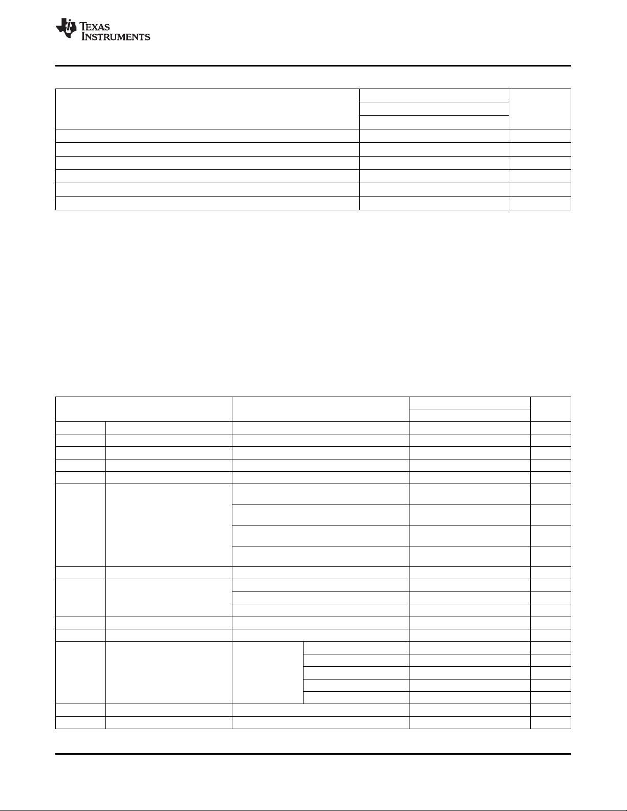
Figure 1. Typical Application Circuit
Crosstalk
• Available in 1.5mm × 1.5mm SON-6 Package
(1)
See the Input and Output Capacitor Requirements in the
Application Information section
1
Please be aware that an important notice concerning availability, standard warranty, and use in critical applications of
Texas Instruments semiconductor products and disclaimers thereto appears at the end of this data sheet.
PRODUCTION DATA information is current as of publication date.
Copyright © 2013, Texas Instruments Incorporated
Products conform to specifications per the terms of the Texas
Instruments standard warranty. Production processing does not
necessarily include testing of all parameters.
TLV7103318-Q1
TLV7101828-Q1
SBVS202A –MARCH 2013–REVISED MARCH 2013
www.ti.com
This integrated circuit can be damaged by ESD. Texas Instruments recommends that all integrated circuits be handled with
appropriate precautions. Failure to observe proper handling and installation procedures can cause damage.
ESD damage can range from subtle performance degradation to complete device failure. Precision integrated circuits may be more
susceptible to damage because very small parametric changes could cause the device not to meet its published specifications.
DEVICE DETAILS
PRODUCT V
OUT
(1)
TLV710xxyyqwwwz XX is nominal output voltage of channel 1 (for example 18 = 1.8 V).
YY is nominal output voltage of channel 2 (for example 28 = 2.8V).
Q is optional. Use "U" for devices with EN pin pull-up resistor, and "D" for devices with EN
pin pull-down resistor.
WWW is package designator.
Z is package quantity. Use "R" for reel (3000 pieces), and "T" for tape (250 pieces).
(1) Output voltages from 1.2V to 4.8V in 50mV increments are available through the use of innovative factory OTP programming; minimum
order quantities may apply. Contact factory for details and availability.
ORDERING INFORMATION
(1)
ORDERABLE PART NUMBER T
A
PACKAGE
(2)
TOP-SIDE MARKING
TLV7103318QDSERQ1 ZD
–40°C to 125°C WSON-DSE Reel of 3000
TLV7101828QDSERQ1 CP
(1) For the most-current package and ordering information, see the Package Option Addendum at the end of this document, or visit the
device product folder on www.ti.com.
(2) Package drawings, thermal data, and symbolization are available at www.ti.com/packaging.
ABSOLUTE MAXIMUM RATINGS
(1)
At T
A
= –40°C to 125°C (unless otherwise noted).
VALUE
MIN MAX UNIT
IN –0.3 6 V
Voltage
(2)
EN –0.3 V
IN
0.3 V
OUT –0.3 6 V
Current OUT Internally limited A
Output short-circuit duration Indefinite s
Operating ambient, T
A
–40 125 °C
Temperature Junction, T
J
150 °C
Storage, T
stg
–55 150 °C
Human-Body Model (HBM) AEC-Q100 Classification Level H2 2 kV
Electrostatic Discharge (ESD) rating
Charged-Device Model (CDM) AEC-Q100 Classification Level
750 V
C4B
(1) Stresses beyond those listed under Absolute Maximum Ratings may cause permanent damage to the device. These are stress ratings
only, and functional operation of the device at these or any other conditions beyond those indicated under Recommended Operating
Conditions is not implied. Exposure to absolute-maximum-rated conditions for extended periods my affect device reliability.
(2) All voltages with respect to ground.
2 Submit Documentation Feedback Copyright © 2013, Texas Instruments Incorporated
Product Folder Links: TLV7103318-Q1 TLV7101828-Q1
TLV7103318-Q1
TLV7101828-Q1
www.ti.com
SBVS202A –MARCH 2013–REVISED MARCH 2013
THERMAL INFORMATION
TLV7103318-Q1, TLV7101828-Q1
THERMAL METRIC
(1)
DSE UNIT
6 PINS
θ
JA
Junction-to-ambient thermal resistance
(2)
190.5 °C/W
θ
JCtop
Junction-to-case (top) thermal resistance
(3)
94.9 °C/W
θ
JB
Junction-to-board thermal resistance
(4)
149.3 °C/W
ψ
JT
Junction-to-top characterization parameter
(5)
6.4 °C/W
ψ
JB
Junction-to-board characterization parameter
(6)
152.8 °C/W
θ
JCbot
Junction-to-case (bottom) thermal resistance
(7)
N/A °C/W
(1) For more information about traditional and new thermal metrics, see the IC Package Thermal Metrics application report, SPRA953.
(2) The junction-to-ambient thermal resistance under natural convection is obtained in a simulation on a JEDEC-standard, high-K board, as
specified in JESD51-7, in an environment described in JESD51-2a.
(3) The junction-to-case (top) thermal resistance is obtained by simulating a cold plate test on the package top. No specific JEDEC-
standard test exists, but a close description can be found in the ANSI SEMI standard G30-88.
(4) The junction-to-board thermal resistance is obtained by simulating in an environment with a ring cold plate fixture to control the PCB
temperature, as described in JESD51-8.
(5) The junction-to-top characterization parameter, ψ
JT
, estimates the junction temperature of a device in a real system and is extracted
from the simulation data for obtaining θ
JA
, using a procedure described in JESD51-2a (sections 6 and 7).
(6) The junction-to-board characterization parameter, ψ
JB
, estimates the junction temperature of a device in a real system and is extracted
from the simulation data for obtaining θ
JA
, using a procedure described in JESD51-2a (sections 6 and 7).
(7) The junction-to-case (bottom) thermal resistance is obtained by simulating a cold plate test on the exposed (power) pad. No specific
JEDEC standard test exists, but a close description can be found in the ANSI SEMI standard G30-88.
Spacer
RECOMMENDED OPERATING CONDITIONS
At T
A
= –40°C to 125ºC, V
IN
= V
OUT(TYP)
+ 0.5 V or 2 V (whichever is greater), I
OUT
= 10 mA, V
EN1
= V
EN2
= 0.9 V, and C
OUT1
=
C
OUT2
= 1 μF, unless otherwise noted.
TLV710xxx8-Q1
PARAMETER TEST CONDITIONS MIN TYP MAX UNIT
V
IN
Input voltage range 2 5.5 V
V
O
Output voltage range 1.2 4.8 V
V
OUT
DC output accuracy –40°C ≤ T
A
≤ 125°C –2 2 %
ΔV
O
/ΔV
IN
Line regulation V
OUT(NOM)
+ 0.5 V ≤ V
IN
≤ 1 5 mV
ΔV
O
/ΔI
OUT
Load regulation 0 mA ≤ I
OUT
≤ 200 mA 5 15 mV
V
IN
= 0.98 V × V
OUT(NOM)
, I
OUT
= 200 mA,
200 285 mV
2V ≤ V
OUT
< 2.4V
V
IN
= 0.98 V × V
OUT(NOM)
, I
OUT
= 200 mA,
175 250 mV
2.4 V ≤ V
OUT
< 2.8 V
V
DO
Dropout voltage
V
IN
= 0.98 V × V
OUT(NOM)
, I
OUT
= 200 mA,
150 215 mV
2.8 V ≤ V
OUT
< 3.3 V
V
IN
= 0.98 V × V
OUT(NOM)
, I
OUT
= 200 mA,
140 200 mV
3.3 V ≤ V
OUT
≤ 4.8 V
I
CL
Output current limit V
OUT
= 0.9V × V
OUT(NOM)
220 350 550 mA
V
EN1
= high, V
EN2
= low, I
OUT1
= 0 mA 35 μA
I
Q
Quiescent current V
EN1
= low, V
EN2
= high, I
OUT2
= 0 mA 35 μA
V
EN1
= high, V
EN2
= high, I
OUT
= 0 mA 70 110 µA
I
GND
Ground pin current I
OUT1
= I
OUT2
= 200mA 360 µA
I
SHUTDOWN
Shutdown current V
EN1,2
≤ 0.4 V, 2 V ≤ V
IN
≤ 4.5 V 2.5 4 μA
f = 10 Hz 80 dB
f = 100 Hz 75 dB
PSRR Power-supply rejection ratio V
OUT
= 1.8 V f = 1k Hz 70 dB
f = 10 kHz 70 dB
f = 100 kHz 50 dB
V
N
Output noise voltage BW = 100 Hz to 100 kHz, V
OUT
= 1.8 V 48 μV
RMS
t
STR
Startup time
(1)
C
OUT
= 1 μF, I
OUT
= 200 mA 100 μs
(1) Startup time = time from EN assertion to 0.98 x V
OUT(NOM)
.
Copyright © 2013, Texas Instruments Incorporated Submit Documentation Feedback 3
Product Folder Links: TLV7103318-Q1 TLV7101828-Q1
TLV7103318-Q1
TLV7101828-Q1
SBVS202A –MARCH 2013–REVISED MARCH 2013
www.ti.com
RECOMMENDED OPERATING CONDITIONS (continued)
At T
A
= –40°C to 125ºC, V
IN
= V
OUT(TYP)
+ 0.5 V or 2 V (whichever is greater), I
OUT
= 10 mA, V
EN1
= V
EN2
= 0.9 V, and C
OUT1
=
C
OUT2
= 1 μF, unless otherwise noted.
TLV710xxx8-Q1
PARAMETER TEST CONDITIONS MIN TYP MAX UNIT
V
HI
Enable high (enabled) 0.9 V
IN
V
V
LO
Enable low (shutdown) 0 0.4 V
TLV7103318-Q1, TLV7101828-Q1 0.04 μA
I
EN
Enable pin current, enabled
TLV710-D 6 μA
UVLO Undervoltage lockout V
IN
rising 1.9 V
T
A
Operating ambient temperature –40 125 °C
Shutdown, temperature increasing 165 °C
T
SD
Thermal shutdown temperature
Reset, temperature decreasing 145 °C
4 Submit Documentation Feedback Copyright © 2013, Texas Instruments Incorporated
Product Folder Links: TLV7103318-Q1 TLV7101828-Q1
Thermal
Shutdown
UVLO
TLV710-D
only
TLV710-D
OUT1
OUT2
EN2
EN1
IN
120W
150kW
Thermal
Shutdown
UVLO
GND
Current
Limit
Current
Limit
Bandgap
Bandgap
Enable
and
Power
Control
Logic
TLV710-D
only
120W
TLV7103318-Q1
TLV7101828-Q1
www.ti.com
SBVS202A –MARCH 2013–REVISED MARCH 2013
FUNCTIONAL BLOCK DIAGRAM
Copyright © 2013, Texas Instruments Incorporated Submit Documentation Feedback 5
Product Folder Links: TLV7103318-Q1 TLV7101828-Q1
剩余26页未读,继续阅读
安全验证
文档复制为VIP权益,开通VIP直接复制
信息提交成功
评论0
最新资源