没有合适的资源?快使用搜索试试~ 我知道了~
TI-TLV840-Q1.pdf
需积分: 10 0 下载量 25 浏览量
2022-11-16
23:00:54
上传
评论 5
收藏 2.08MB PDF 举报
温馨提示
试读
32页
TI-TLV840-Q1.pdf
资源推荐
资源详情
资源评论
TLV840-Q1 Nano-Power Voltage Supervisor with Adjustable Reset Time Delay
1 Features
Qualified for automotive applications:
• AEC-Q100 qualified with the following results:
– Device temperature grade 1: –40°C to +125°C
ambient operating temperature
– Device HBM ESD classification level 2
– Device CDM ESD classification level C7B
Designed for high performance:
• Nano supply current : 120 nA (Typ)
• High accuracy: ±0.5% (Typ)
• Built-in hysteresis (V
HYS
): 5% (Typ)
• Fixed threshold voltage (V
IT-
): 0.8 V to 5.4 V
Designed for a wide range of applications:
• Operating voltage range : 0.7 V to 6 V
• Fixed (V
IT-
) voltage: 0.8 V to 5.4 V in 0.1 V steps
• Programmable reset time delay (t
D
)
– Min time delay: 40 µs (typ) without capacitor
• Active-low manual reset (MR)
Multiple output topologies / Package type:
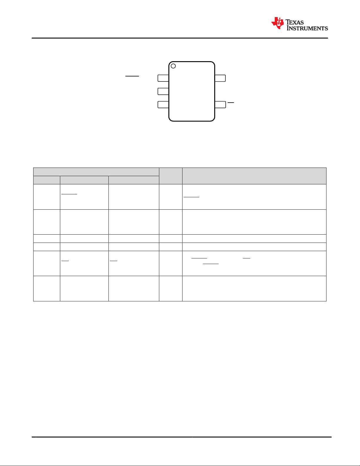
• Four output topologies (RESET / RESET):
– TLV840MADL-Q1: open-drain, active-low
– TLV840MAPL-Q1: push-pull, active-low
– TLV840MADH-Q1: open-drain, active-high
– TLV840MAPH-Q1: push-pull, active-high
• Package: SOT23-5 (DBV)
2 Applications
• Surround view system, front camera
• Automotive gateway
• Radar ECU
• Automotive head unit
• ADAS controller
• Emergency call
• Telematics control unit
3 Description
The TLV840-Q1 device is a voltage supervisor or
reset IC that can operate at wide input voltage levels
from 0.7 V to 6 V while maintaining very low quiescent
current across the whole VDD and temperature range.
TLV840-Q1 offers the best combination of low power
consumption, high accuracy and low propagation
delay (t
p_HL
= 30 µs typical).
Reset output signal is asserted when the voltage at
VDD drops below the negative voltage threshold
(V
IT-
). Reset signal is cleared when VDD rise above
V
IT-
plus hysteresis (V
HYS
) and the reset time delay
(t
D
) expires. Reset time delay can be programmed
by connecting a capacitor between the CT pin and
ground. For a minimum reset delay time the CT pin
can be left floating. The TLV840-Q1, with its manual
reset pin (MR), offers program flexibility by forcing the
system into a hard reset when the pin is asserted.
Additional features: Low power-on reset voltage
(V
POR
), built-in glitch immunity protection for VDD,
built-in hysteresis, low open-drain output leakage
current (I
lkg(OD)
). TLV840-Q1 is a perfect voltage
monitoring solution for automotive applications and
battery-powered / low-power applications.
Device Information
PART NUMBER PACKAGE
(1)
BODY SIZE (NOM)
TLV840-Q1 SOT-23 (5) (DBV) 2.90 mm × 1.60 mm
(1) For package details, see the mechanical drawing addendum
at the end of the data sheet.
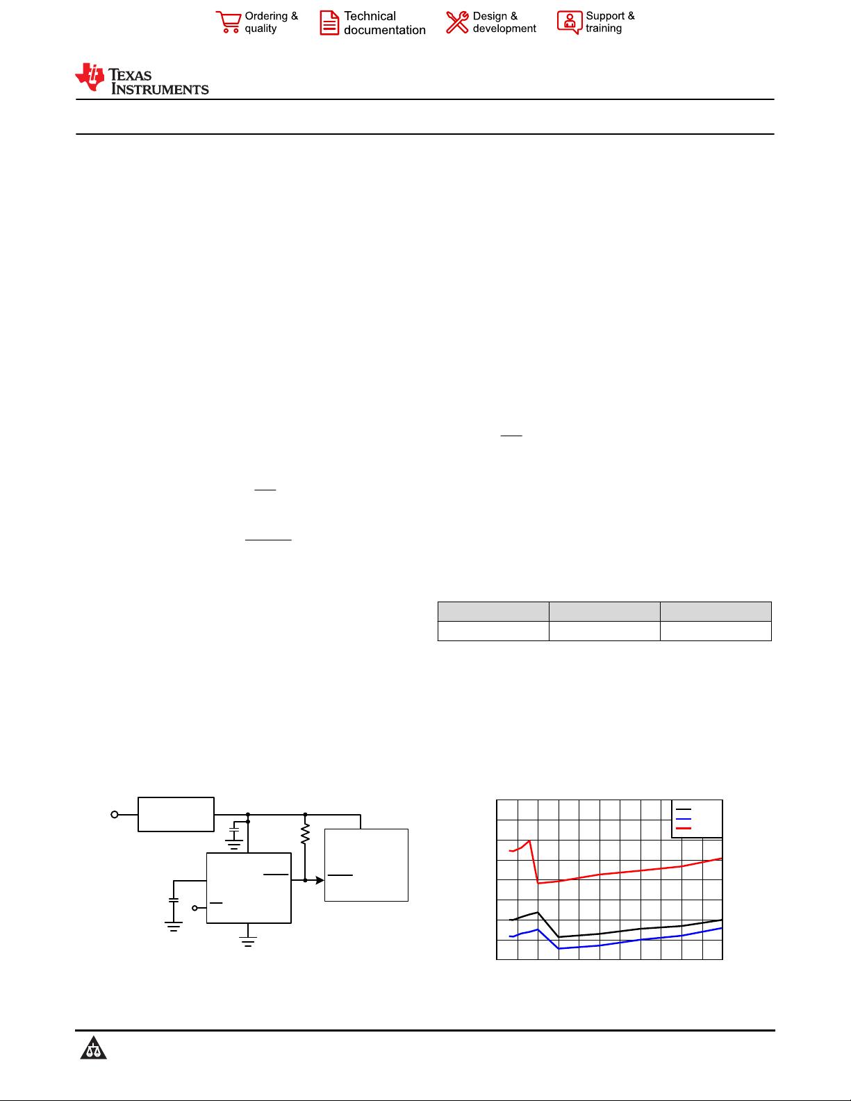
TLV840MADL29Q1
VDD
GND
RESET
Microcontroller
VDD
5 V
RESET
LDO
3.3 V
CT
IN
OUT
*R
pu
*R
pu
only for open-drain output
MR
Typical Application Circuit
V
DD
(V)
I
DD
(µA)
0.5 1 1.5 2 2.5 3 3.5 4 4.5 5 5.5 6
0.08
0.12
0.16
0.2
0.24
0.28
0.32
0.36
0.4
IDDv
25°C
-40°C
125°C
Typical Supply Current
www.ti.com
TLV840-Q1
SNVSBY3A – NOVEMBER 2020 – REVISED APRIL 2021
Copyright © 2021 Texas Instruments Incorporated
Submit Document Feedback
1
Product Folder Links: TLV840-Q1
TLV840-Q1
SNVSBY3A – NOVEMBER 2020 – REVISED APRIL 2021
An IMPORTANT NOTICE at the end of this data sheet addresses availability, warranty, changes, use in safety-critical applications,
intellectual property matters and other important disclaimers. PRODUCTION DATA.
Table of Contents
1 Features............................................................................1
2 Applications..................................................................... 1
3 Description.......................................................................1
4 Revision History.............................................................. 2
5 Device Comparison......................................................... 3
6 Pin Configuration and Functions...................................4
7 Specifications.................................................................. 5
7.1 Absolute Maximum Ratings ....................................... 5
7.2 ESD Ratings .............................................................. 5
7.3 Recommended Operating Conditions ........................5
7.4 Thermal Information ...................................................5
7.5 Electrical Characteristics ............................................6
7.6 Timing Requirements ................................................. 7
7.7 Timing Diagrams ........................................................ 8
7.8 Typical Characteristics ............................................. 10
8 Detailed Description......................................................12
8.1 Overview................................................................... 12
8.2 Functional Block Diagram......................................... 12
8.3 Feature Description...................................................12
8.4 Device Functional Modes..........................................17
9 Application and Implementation.................................. 18
9.1 Application Information............................................. 18
9.2 Typical Application.................................................... 18
10 Power Supply Recommendations..............................21
11 Layout........................................................................... 22
11.1 Layout Guidelines................................................... 22
11.2 Layout Example...................................................... 22
12 Device and Documentation Support..........................23
12.1 Device Nomenclature..............................................23
12.2 Receiving Notification of Documentation Updates..24
12.3 Support Resources................................................. 24
12.4 Trademarks............................................................. 24
13 Mechanical, Packaging, and Orderable
Information.................................................................... 24
4 Revision History
Changes from Revision * (November 2020) to Revision A (April 2021) Page
• RTM release....................................................................................................................................................... 1
TLV840-Q1
SNVSBY3A – NOVEMBER 2020 – REVISED APRIL 2021
www.ti.com
2 Submit Document Feedback
Copyright © 2021 Texas Instruments Incorporated
Product Folder Links: TLV840-Q1
5 Device Comparison
Figure 5-1 shows the device naming nomenclature to compare the different device variants. See Section 12.1 for
a more detailed explanation.
TLV 840 X X XX XX XXX
Feature Op
on
M: Capacitor delay (CT)
and manual reset (MR)
Output Type
DL: Open-drain,
ac
ve-low
PL: Push-pull,
ac
ve-low
DH: Open-drain,
ac
ve-high
PH: Push-pull,
ac
ve-high
Detect Voltage Threshold
08: 0.8V
...
54: 5.4V
Delay Op
on
A:
- 40 µs default
(CT pin
oa
ng)
- Programmable
(CT pin with capacitor
to GND)
Package
DBV: SOT23
Q1
Figure 5-1. Device Naming Nomenclature
www.ti.com
TLV840-Q1
SNVSBY3A – NOVEMBER 2020 – REVISED APRIL 2021
Copyright © 2021 Texas Instruments Incorporated
Submit Document Feedback
3
Product Folder Links: TLV840-Q1
6 Pin Configuration and Functions
1
2VDD
3GND 4
5
CT
Not to scale
MR
RESET / RESET
Figure 6-1. Pin Configuration TLV840M-Q1
DBV Package 5-Pin SOT-23
TLV840M-Q1 Top View
Table 6-1. Pin Functions
PIN
I/O DESCRIPTION
PIN NO. TLV840MAxL-Q1 TLV840MAxH-Q1
1 RESET N/A O
Active-Low Output Reset Signal: This pin is driven logic low
when VDD voltage falls below the negative voltage threshold (V
IT-
).
RESET remains low (asserted) for the delay time period (t
D
) after
VDD voltage rises above V
IT+
= V
IT-
+V
HYS
.
1 N/A RESET O
Active-High Output Reset Signal: This pin is driven logic high
when VDD voltage falls below the negative voltage threshold (V
IT-
).
RESET remains high (asserted) for the delay time period (t
D
) after
VDD voltage rises above V
IT+
= V
IT-
+V
HYS
.
2 VDD VDD I Input Supply Voltage: TLV840-Q1 monitors VDD voltage
3 GND GND _ Ground
4 MR MR I
Manual Reset: Pull this pin to a logic low to assert a reset signal in
the RESET output pin. After MR pin is left floating or pulls to logic
high, the RESET output deasserts to the nominal state after the
reset delay time (t
D
) expires.
5 CT CT -
Capacitor Time Delay Pin: The CT pin offers a user-
programmable delay time. Connect an external capacitor on this
pin to adjust time delay. When not in use leave pin floating for the
smallest fixed time delay.
TLV840-Q1
SNVSBY3A – NOVEMBER 2020 – REVISED APRIL 2021
www.ti.com
4 Submit Document Feedback
Copyright © 2021 Texas Instruments Incorporated
Product Folder Links: TLV840-Q1
7 Specifications
7.1 Absolute Maximum Ratings
over operating free-air temperature range, unless otherwise noted
(1)
MIN MAX UNIT
Voltage VDD –0.3 6.5 V
Voltage
CT, MR
(2)
, RESET (TLV840MAPL), RESET
(TLV840MAPH)
–0.3 V
DD
+0.3
(3)
V
RESET (TLV840MADL) –0.3 6.5
Current RESET, RESET pin –20 20 mA
Temperature
(4)
Operating ambient temperature, T
A
–40 125
℃
Temperature
(4)
Storage, T
stg
–65 150
(1) Stresses beyond those listed under Absolute Maximum Rating may cause permanent damage to the device. These are stress
ratings only, which do not imply functional operation of the device at these or any other conditions beyond those indicated
under Recommended Operating Condition. Exposure to absolute-maximum-rated conditions for extended periods may affect device
reliability.
(2) If the logic signal driving MR is less than VDD, then I
DD
current increases based on voltage differential.
(3) The absolute maximum rating is (VDD + 0.3) V or 6.5 V, whichever is smaller
(4) As a result of the low dissipated power in this device, it is assumed that T
J
= T
A
.
7.2 ESD Ratings
VALUE
UNIT
V
(ESD)
Electrostatic discharge
Human body model (HBM), per AEC Q100-002
(1)
±2000
V
Charged device model (CDM), per AEC Q100-011 ±750
(1) AEC Q100-002 indicates that HBM stressing shall be in accordance with the ANSI/ESDA/JEDEC JS-001 specification.
7.3 Recommended Operating Conditions
over operating free-air temperature range (unless otherwise noted)
MIN NOM MAX UNIT
Voltage
VDD (TLV840MAxL) 0.7 6
V
CT, RESET (TLV840MAxL), RESET (TLV840MAPH) ,
MR
0 6
Current RESET and RESET pin current –5 5 mA
T
A
Operating ambient temperature –40 125 ℃
7.4 Thermal Information
THERMAL METRIC
(1)
TLV840-Q1
UNITDBV (SOT23-5)
5 PINS
R
θJA
Junction-to-ambient thermal resistance 193.5 °C/W
R
θJC(top)
Junction-to-case (top) thermal resistance 117.9 °C/W
R
θJB
Junction-to-board thermal resistance 98.5 °C/W
ψ
JT
Junction-to-top characterization parameter 43.4 °C/W
ψ
JB
Junction-to-board characterization parameter 97.8 °C/W
R
θJC(bot)
Junction-to-case (bottom) thermal resistance N/A °C/W
(1) For more information about traditional and new thermal metrics, see the Semiconductor and IC Package Thermal Metrics application
report.
www.ti.com
TLV840-Q1
SNVSBY3A – NOVEMBER 2020 – REVISED APRIL 2021
Copyright © 2021 Texas Instruments Incorporated
Submit Document Feedback
5
Product Folder Links: TLV840-Q1
剩余31页未读,继续阅读
资源评论
不觉明了
- 粉丝: 3163
- 资源: 5419
上传资源 快速赚钱
- 我的内容管理 展开
- 我的资源 快来上传第一个资源
- 我的收益 登录查看自己的收益
- 我的积分 登录查看自己的积分
- 我的C币 登录后查看C币余额
- 我的收藏
- 我的下载
- 下载帮助
安全验证
文档复制为VIP权益,开通VIP直接复制
信息提交成功