TI-TLV431B-Q1.pdf
需积分: 9 150 浏览量
2022-11-20
16:47:58
上传
评论 5
收藏 1.5MB PDF 举报

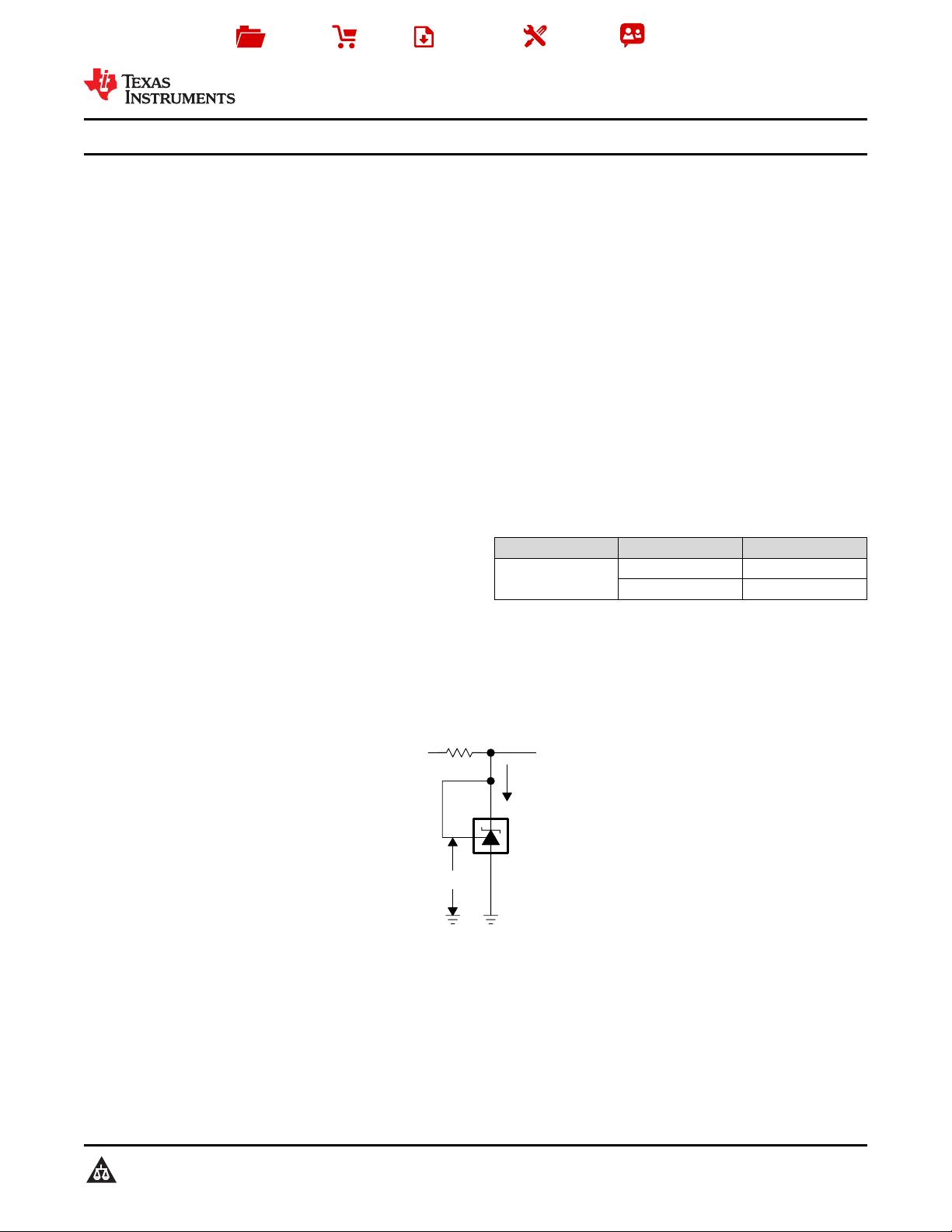
V
REF
Input
V
I
O
K
Product
Folder
Order
Now
Technical
Documents
Tools &
Software
Support &
Community
An IMPORTANT NOTICE at the end of this data sheet addresses availability, warranty, changes, use in safety-critical applications,
intellectual property matters and other important disclaimers. PRODUCTION DATA.
TLV431A-Q1
,
TLV431B-Q1
SLVS905A –DECEMBER 2008–REVISED OCTOBER 2017
TLV431x-Q1 Low-Voltage Adjustable Precision Shunt Regulator
1
1 Features
1
• Qualified for Automotive Applications
• AEC-Q100 Qualified With the Following Results:
– Device Temperature Grade 1: -40°C to 125°C
Ambient Operating Temperature Range
• Low-Voltage Operation, V
REF
= 1.24 V
• Adjustable Output Voltage, V
O
= V
REF
to 6 V
• Reference Voltage Tolerances at 25°C
– 0.5% for TLV431B
– 1% for TLV431A
• Typical Temperature Drift
– 11 mV (–40°C to 125°C)
• Low Operational Cathode Current, 80 µA Typ
• 0.25-Ω Typical Output Impedance
• See TLVH431 and TLVH432 for:
– Wider V
KA
(1.24 V to 18 V) and I
K
(80 mA)
– Multiple Pinouts for SOT-23-3 and SOT-89
Packages
2 Applications
• Adjustable Voltage and Current Referencing
• Secondary Side Regulation in Flyback SMPSs
• Zener Replacement
• Voltage Monitoring
• Comparator with Integrated Reference
3 Description
The TLV431 device is a low-voltage 3-terminal
adjustable voltage reference with specified thermal
stability over applicable industrial and commercial
temperature ranges. Output voltage can be set to
1.24V on stand alone mode or any value between
V
REF
(1.24 V) and 6 V with two external resistors (see
Figure 23). These devices operate from a lower
voltage (1.24 V) than the widely used TL431 and
TL1431 shunt-regulator references.
When used with an optocoupler, the TLV431 device
is an ideal voltage reference in isolated feedback
circuits for 3-V to 3.3-V switching-mode power
supplies. These devices have a typical output
impedance of 0.25 Ω. Active output circuitry provides
a very sharp turn-on characteristic, making them
excellent replacements for low-voltage Zener diodes
in many applications, including on-board regulation
and adjustable power supplies.
Device Information
(1)
PART NUMBER PACKAGE (PIN) BODY SIZE (NOM)
TLV431x-Q1
SOT-23 (3) 2.90 mm x 1.30 mm
SOT-23 (5) 2.90 mm x 1.60 mm
(1) For all available packages, see the orderable addendum at
the end of the data sheet.
Simplified Schematic


剩余35页未读,继续阅读
资源评论


不觉明了
- 粉丝: 3163
- 资源: 5419


