没有合适的资源?快使用搜索试试~ 我知道了~
TI-TLV5535-Q1.pdf
需积分: 5 0 下载量 135 浏览量
2022-11-27
16:19:37
上传
评论 4
收藏 698KB PDF 举报
温馨提示
试读
37页
TI-TLV5535-Q1.pdf
资源详情
资源评论
SGLS230A − JANUARY 2004 − REVISED JUNE 2008
1
POST OFFICE BOX 655303 • DALLAS, TEXAS 75265
D Meets AEC-Q100-011 C3A CDM
Classification
D Qualified for Automotive Applications
D 8-Bit Resolution, 35 MSPS Sampling
Analog-to-Digital Converter (ADC)
D Low Power Consumption: 90 mW Typ
Using External References
D Wide Analog Input Bandwidth: 600 MHz Typ
D 3.3-V Single-Supply Operation
D 3.3-V TTL/CMOS-Compatible Digital I/O
D Internal Bottom and Top Reference
Voltages
D Adjustable Reference Input Range
D Power-Down (Standby) Mode
D Separate Power Down for Internal Voltage
References
D Three-State Outputs
D 28-Pin Thin Shrink SOP (TSSOP) Packages
D Applications
− Digital Communications (IF Sampling)
− High-Speed DSP Front-End
(TMS320C6000)
− Video Processing (Scan Rate/Format
Conversion)
− DVD Read Channel Digitization
description/ordering information
The TLV5535 is an 8-bit, 35 MSPS, high-speed A/D converter. It converts the analog input signal into 8-bit
binary-coded digital words up to a sampling rate of 35 MHz. All digital inputs and outputs are 3.3 V
TTL/CMOS-compatible.
The device consumes very little power due to the 3.3-V supply and an innovative single-pipeline architecture
implemented in a CMOS process. The user obtains maximum flexibility by setting both bottom and top voltage
references from user-supplied voltages. If no external references are available, on-chip references are
available for internal and external use. The full-scale range is 1 V
pp
up to 1.6 V
pp
, depending on the analog
supply voltage. If external references are available, the internal references can be disabled independently from
the rest of the chip, resulting in an even greater power saving.
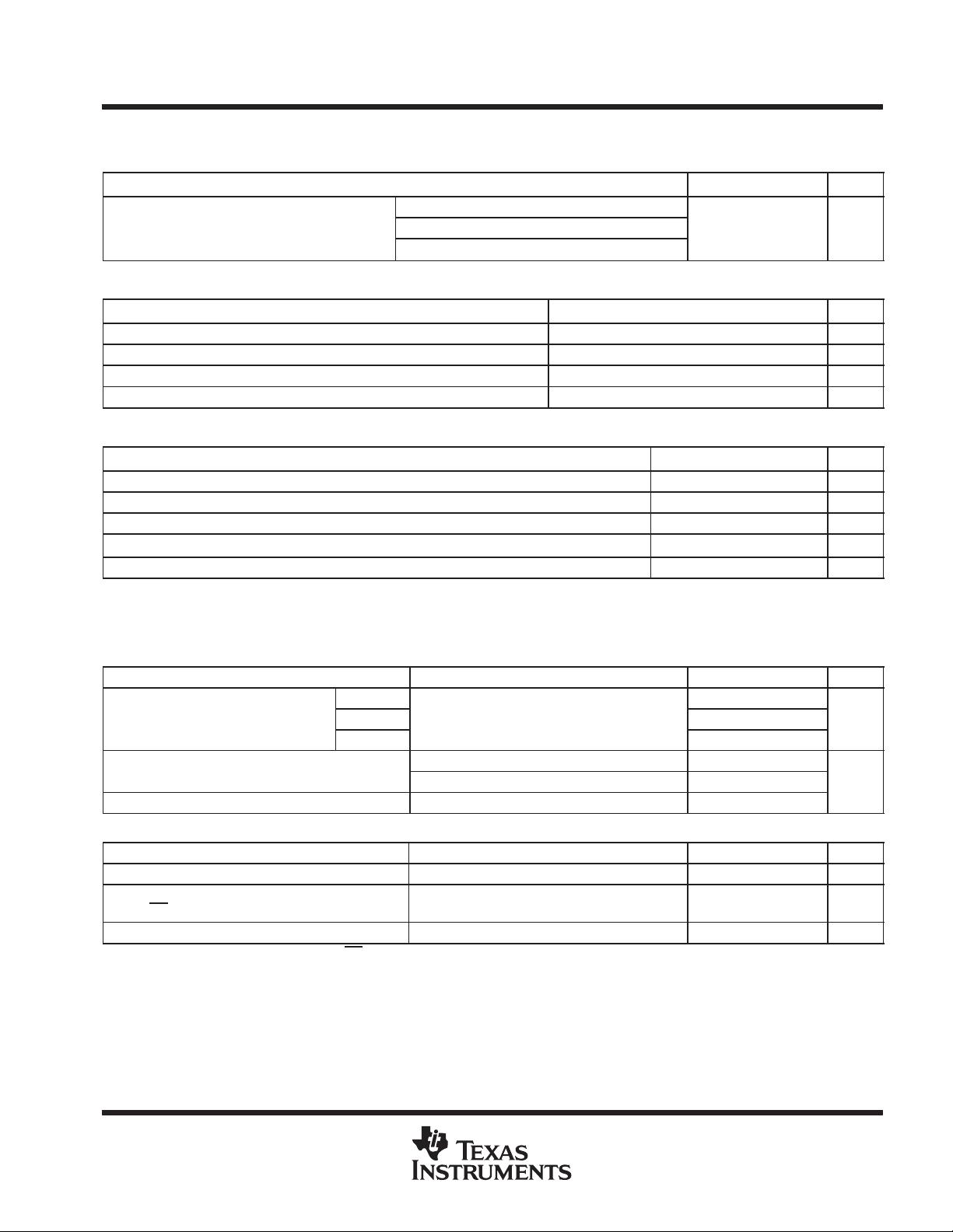
ORDERING INFORMATION
{
T
J
PACKAGE
}
ORDERABLE
PART NUMBER
TOP-SIDE
MARKING
−40°C to 85°C TSSOP (PW) Tape and reel TLV5535IPWRQ1 TLV5535Q1
†
For the most current package and ordering information, see the Package Option Addendum at the end
of this document, or see the TI web site at http://www.ti.com.
‡
Package drawings, thermal data, and symbolization are available at http://www.ti.com/packaging.
Copyright 2008 Texas Instruments Incorporated
!" # $%&" !# '%()$!" *!"&+
*%$"# $ " #'&$$!"# '& ",& "&# &-!# #"%&"#
#"!*!* .!!"/+ *%$" '$&##0 *&# " &$&##!)/ $)%*&
"&#"0 !)) '!!&"&#+
Please be aware that an important notice concerning availability, standard warranty, and use in critical applications of
Texas Instruments semiconductor products and disclaimers thereto appears at the end of this data sheet.
1
2
3
4
5
6
7
8
9
10
11
12
13
14
28
27
26
25
24
23
22
21
20
19
18
17
16
15
DRV
DD
D0
D1
D2
D3
D4
D5
D6
D7
DRV
SS
DV
SS
CLK
OE
DV
DD
AV
SS
AV
DD
AIN
CML
PWDN_REF
AV
SS
REFBO
REFBI
REFTI
REFTO
AV
SS
BG
AV
DD
STBY
PW PACKAGE
(TOP VIEW)
SGLS230A − JANUARY 2004 − REVISED JUNE 2008
2
POST OFFICE BOX 655303 • DALLAS, TEXAS 75265
description (continued)
While usable in a wide variety of applications, the device is specifically suited for the digitizing of high-speed
graphics and for interfacing to LCD panels or LCD/DMD projection modules . Other applications include DVD
read channel digitization, medical imaging, and communications. This device is suitable for IF sampling of
communication systems using sub-Nyquist sampling methods because of its high analog input bandwidth.
functional block diagram
SHA
DACADC
+
−
ADC
Correction Logic
Output Buffers
2222 2
D0(LSB)−D7(MSB)
2
2
SHA SHA SHA SHA SHA
The single-pipeline architecture uses 6 ADC/DAC stages and one final flash ADC. Each stage produces a
resolution of 2 bits. The correction logic generates its result using the 2-bit result from the first stage, 1 bit from
each of the 5 succeeding stages, and 1 bit from the final stage in order to arrive at an 8-bit result. The correction
logic ensures no missing codes over the full operating temperature range.
SGLS230A − JANUARY 2004 − REVISED JUNE 2008
3
POST OFFICE BOX 655303 • DALLAS, TEXAS 75265
circuit diagrams of inputs and outputs
DV
DD
AV
DD
AV
DD
0.5 pF
Internal
Reference
Generator
REFTO
or
REFBO
AV
DD
REFBI
or
REFTI
OE
ALL DIGITAL INPUT CIRCUITS AIN INPUT CIRCUIT
REFERENCE INPUT CIRCUIT D0−D7 OUTPUT CIRCUIT
DRV
DD
DRV
SS
D_Out
D
SGLS230A − JANUARY 2004 − REVISED JUNE 2008
4
POST OFFICE BOX 655303 • DALLAS, TEXAS 75265
Terminal Functions
TERMINAL
I/O
DESCRIPTION
NAME NO.
I/O
DESCRIPTION
AIN 26 I Analog input
AV
DD
16, 27 I Analog supply voltage
AV
SS
18, 23, 28 I Analog ground
BG 17 O Band gap reference voltage. A 1-µF capacitor (with an optional 0.1-µF capacitor in parallel) should be
connected between this terminal and AV
SS
for external filtering.
CLK 12 I Clock input. The input is sampled on each rising edge of CLK.
CML 25 O Common mode level. This voltage is equal to (AV
DD
− AV
SS
) ÷ 2. An external 0.1-µF capacitor should be
connected between this terminal and AV
SS
.
D0 − D7 2 − 9 O Data outputs. D7 is the MSB.
DRV
DD
1 I Supply voltage for digital output drivers
DRV
SS
10 I Ground for digital output drivers
DV
DD
14 I Digital supply voltage
OE 13 I Output enable. When high, the D0 − D7 outputs go in high-impedance mode.
DV
SS
11 I Digital ground
PWDN_REF 24 I Power down for internal reference voltages. A high on this terminal disables the internal reference circuit.
REFBI 21 I Reference voltage bottom input. The voltage at this terminal defines the bottom reference voltage for the
ADC. It can be connected to REFBO or to an externally generated reference level. Sufficient filtering
should be applied to this input. The use of a 0.1-µF capacitor connected between REFBI and AV
SS
is
recommended. Additionaly, a 0.1-µF capacitor can be connected between REFTI and REFBI.
REFBO 22 O Reference voltage bottom output. An internally generated reference is available at this terminal. It can be
connected to REFBI or left unconnected. A 1-µF capacitor between REFBO and AV
SS
provides sufficient
decoupling required for this output.
REFTI 20 I Reference voltage top input. The voltage at this terminal defines the top reference voltage for the ADC.
It can be connected to REFTO or to an externally generated reference level. Sufficient filtering should be
applied to this input. The use of a 0.1-µF capacitor between REFTI and AV
SS
is recommended.
Additionaly, a 0.1-µF capacitor can be connected between REFTI and REFBI.
REFTO 19 O Reference voltage top output. An internally generated reference is available at this terminal. It can be
connected to REFTI or left unconnected. A 1-µF capacitor between REFTO and AV
SS
provides sufficient
decoupling required for this output.
STBY 15 I Standby input. A high level on this input enables power-down mode.
absolute maximum ratings over operating free-air temperature (unless otherwise noted)
†
Supply voltage range: AV
DD
to AV
SS
, DV
DD
to DV
SS
−0.5 V to 4.5 V. . . . . . . . . . . . . . . . . . . . . . . . . . . . . . . . . .
AV
DD
to DV
DD
, AV
SS
to DV
SS
−0.5 V to 0.5 V. . . . . . . . . . . . . . . . . . . . . . . . . . . . . . . . . .
Digital input voltage range to DV
SS
−0.5 V to DV
DD
+ 0.5 V. . . . . . . . . . . . . . . . . . . . . . . . . . . . . . . . . . . . . . . . . .
Analog input voltage range to AV
SS
−0.5 V to AV
DD
+ 0.5 V. . . . . . . . . . . . . . . . . . . . . . . . . . . . . . . . . . . . . . . . .
Digital output voltage range applied from external source to DGND −0.5 V to DV
DD
+ 0.5 V. . . . . . . . . . . . . .
Reference voltage input range to AGND: V
(REFTI)
, V
(REFTO)
, V
(REFBI)
, V
(REFBO)
−0.5 V to AV
DD
+ 0.5 V
Operating free-air temperature range, T
A
: TLV5535I −40°C to 85°C. . . . . . . . . . . . . . . . . . . . . . . . . . . . . . . . . .
Storage temperature range, T
stg
−55°C to 150°C. . . . . . . . . . . . . . . . . . . . . . . . . . . . . . . . . . . . . . . . . . . . . . . . . . .
†
Stresses beyond those listed under “absolute maximum ratings” may cause permanent damage to the device. These are stress ratings only, and
functional operation of the device at these or any other conditions beyond those indicated under “recommended operating conditions” is not
implied. Exposure to absolute-maximum-rated conditions for extended periods may affect device reliability.
SGLS230A − JANUARY 2004 − REVISED JUNE 2008
5
POST OFFICE BOX 655303 • DALLAS, TEXAS 75265
recommended operating conditions over operating free-temperature range
power supply
MIN NOM MAX UNIT
AV
DD
− AV
SS
Supply voltage
DV
DD
− DV
SS
3 3.3 3.6 V
Supply voltage
DRV
DD
− DRV
SS
3
3.3
3.6
V
analog and reference inputs
MIN NOM MAX UNIT
Reference input voltage (top), V
(REFTI)
(NOM) − 0.2 2 + (AV
DD
− 3) (NOM) + 0.2 V
Reference input voltage (bottom), V
(REFBI)
0.8 1 1.2 V
Reference voltage differential, V
(REFTI)
− V
(REFBI)
1 + (AV
DD
− 3) V
Analog input voltage, V
(AIN)
V
(REFBI)
V
(REFTI)
V
digital inputs
MIN NOM MAX UNIT
High-level input voltage, V
IH
2.0 DV
DD
V
Low-level input voltage, V
IL
DGND 0.2xDV
DD
V
Clock period, t
c
28.6 ns
Pulse duration, clock high, t
w(CLKH)
13 ns
Pulse duration, clock low, t
w(CLKL)
13 ns
electrical characteristics over recommended operating conditions, f
CLK
= 35 MSPS, external
voltage references (unless otherwise noted)
power supply
PARAMETER TEST CONDITIONS MIN TYP MAX UNIT
AV
DD
AV
DD
= DV
DD
= 3.3 V, DRV
DD
= 3 V,
27 34
I
DD
Operating supply current
DV
DD
AV
DD
= DV
DD
= 3.3 V, DRV
DD
= 3 V,
C
L
= 15 pF, V
I
= 1 MHz, −1-dB FS
1.5 2.6
mA
I
DD
Operating supply current
DRV
DD
C
L
= 15 pF, V
I
= 1 MHz, −1-dB FS
4 6
mA
P
D
Power dissipation
PWDN_REF = L 106 139
P
D
Power dissipation
PWDN_REF = H
90 113
mW
P
D(STBY)
Standby power STBY = H, CLK held high or low 11 15
mW
digital logic inputs
PARAMETER TEST CONDITIONS MIN TYP MAX UNIT
I
IH
High-level input current on CLK
†
AV
DD
= DV
DD
= DRV
DD
= CLK = 3.6 V 10 µA
I
IL
Low-level input current on digital inputs
(OE
, STDBY, PWDN_REF, CLK)
AV
DD
= DV
DD
= DRV
DD
= 3.6 V,
Digital inputs at 0 V
10 µA
C
I
Input capacitance 5 pF
†
I
IH
leakage current on other digital inputs (OE
, STDBY, PWDN_REF) is not measured since these inputs have an internal pull-down resistor of
4 KΩ to DGND.
剩余36页未读,继续阅读
安全验证
文档复制为VIP权益,开通VIP直接复制
信息提交成功
评论0
最新资源