没有合适的资源?快使用搜索试试~ 我知道了~
TI-TLV5535.pdf
需积分: 5 0 下载量 105 浏览量
2022-11-27
16:19:51
上传
评论 4
收藏 1.13MB PDF 举报
温馨提示
试读
36页
TI-TLV5535.pdf
资源推荐
资源详情
资源评论
TLV5535
8-BIT, 35 MSPS, LOW-POWER ANALOG-TO-DIGITAL CONVERTER
SLAS221 – JUNE 1999
1
POST OFFICE BOX 655303 • DALLAS, TEXAS 75265
D
8-Bit Resolution, 35 MSPS Sampling
Analog-to-Digital Converter (ADC)
D
Low Power Consumption: 90 mW Typ
Using External References
D
Wide Analog Input Bandwidth: 600 MHz Typ
D
3.3-V Single-Supply Operation
D
3.3-V TTL/CMOS-Compatible Digital I/O
D
Internal Bottom and Top Reference
Voltages
D
Adjustable Reference Input Range
D
Power-Down (Standby) Mode
D
Separate Power Down for Internal Voltage
References
D
Three-State Outputs
D
28-Pin Thin Shrink SOP (TSSOP) Packages
D
Applications
– Digital Communications (IF Sampling)
– High-Speed DSP Front-End
(TMS320C6000)
– Medical Imaging
– Video Processing (Scan Rate/Format
Conversion)
– DVD Read Channel Digitization
description
The TLV5535 is an 8-bit, 35 MSPS, high-speed A/D converter. It converts the analog input signal into 8-bit
binary-coded digital words up to a sampling rate of 35 MHz. All digital inputs and outputs are 3.3 V
TTL/CMOS-compatible.
The device consumes very little power due to the 3.3-V supply and an innovative single-pipeline architecture
implemented in a CMOS process. The user obtains maximum flexibility by setting both bottom and top voltage
references from user-supplied voltages. If no external references are available, on-chip references are
available for internal and external use. The full-scale range is 1 V
pp
up to 1.6 V
pp
, depending on the analog
supply voltage. If external references are available, the internal references can be disabled independently from
the rest of the chip, resulting in an even greater power saving.
While usable in a wide variety of applications, the device is specifically suited for the digitizing of high-speed
graphics and for interfacing to LCD panels or LCD/DMD projection modules . Other applications include DVD
read channel digitization, medical imaging, and communications. This device is suitable for IF sampling of
communication systems using sub-Nyquist sampling methods because of its high analog input bandwidth.
AVAILABLE OPTIONS
T
A
PACKAGED DEVICES
T
A
TSSOP-28
–40°C to 85°C TLV5535IPW
PRODUCTION DATA information is current as of publication date.
Products conform to specifications per the terms of Texas Instruments
standard warranty. Production processing does not necessarily include
testing of all parameters.
Please be aware that an important notice concerning availability, standard warranty, and use in critical applications of
Texas Instruments semiconductor products and disclaimers thereto appears at the end of this data sheet.
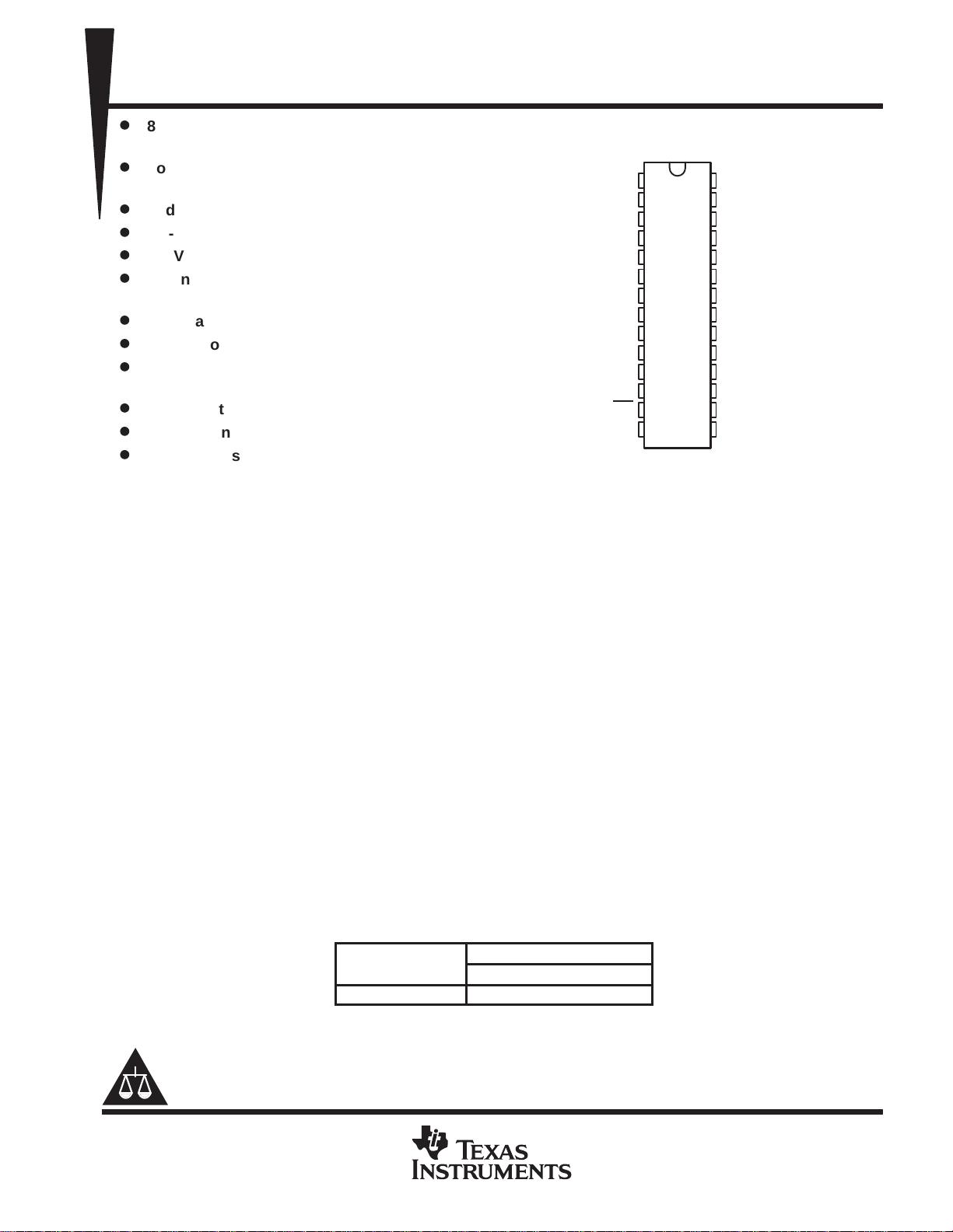
1
2
3
4
5
6
7
8
9
10
11
12
13
14
28
27
26
25
24
23
22
21
20
19
18
17
16
15
DRV
DD
D0
D1
D2
D3
D4
D5
D6
D7
DRV
SS
DV
SS
CLK
OE
DV
DD
AV
SS
AV
DD
AIN
CML
PWDN_REF
AV
SS
REFBO
REFBI
REFTI
REFTO
AV
SS
BG
AV
DD
STBY
PW PACKAGE
(TOP VIEW)
Copyright 1999, Texas Instruments Incorporated
TLV5535
8-BIT, 35 MSPS, LOW-POWER ANALOG-TO-DIGITAL CONVERTER
SLAS221 – JUNE 1999
2
POST OFFICE BOX 655303 • DALLAS, TEXAS 75265
functional block diagram
SHA
DACADC
+
–
ADC
Correction Logic
Output Buffers
2222 2
D0(LSB)–D7(MSB)
2
2
SHA SHA SHA SHA SHA
The single-pipeline architecture uses 6 ADC/DAC stages and one final flash ADC. Each stage produces a
resolution of 2 bits. The correction logic generates its result using the 2-bit result from the first stage, 1 bit from
each of the 5 succeeding stages, and 1 bit from the final stage in order to arrive at an 8-bit result. The correction
logic ensures no missing codes over the full operating temperature range.
circuit diagrams of inputs and outputs
DV
DD
AV
DD
AV
DD
0.5 pF
Internal
Reference
Generator
REFTO
or
REFBO
AV
DD
REFBI
or
REFTI
OE
ALL DIGITAL INPUT CIRCUITS AIN INPUT CIRCUIT
REFERENCE INPUT CIRCUIT D0–D7 OUTPUT CIRCUIT
DRV
DD
DRV
SS
D_Out
D
TLV5535
8-BIT, 35 MSPS, LOW-POWER ANALOG-TO-DIGITAL CONVERTER
SLAS221 – JUNE 1999
3
POST OFFICE BOX 655303 • DALLAS, TEXAS 75265
Terminal Functions
TERMINAL
I/O
DESCRIPTION
NAME NO.
I/O
DESCRIPTION
AIN 26 I Analog input
AV
DD
16, 27 I Analog supply voltage
AV
SS
18, 23, 28 I Analog ground
BG 17 O Band gap reference voltage. A 1-µF capacitor (with an optional 0.1-µF capacitor in parallel) should be
connected between this terminal and AV
SS
for external filtering.
CLK 12 I Clock input. The input is sampled on each rising edge of CLK.
CML 25 O Common mode level. This voltage is equal to (AV
DD
– AV
SS
) ÷ 2. An external 0.1-µF capacitor should be
connected between this terminal and AV
SS
.
D0 – D7 2 – 9 O Data outputs. D7 is the MSB.
DRV
DD
1 I Supply voltage for digital output drivers
DRV
SS
10 I Ground for digital output drivers
DV
DD
14 I Digital supply voltage
OE 13 I Output enable. When high, the D0 – D7 outputs go in high-impedance mode.
DV
SS
11 I Digital ground
PWDN_REF 24 I Power down for internal reference voltages. A high on this terminal disables the internal reference circuit.
REFBI 21 I Reference voltage bottom input. The voltage at this terminal defines the bottom reference voltage for the
ADC. It can be connected to REFBO or to an externally generated reference level. Sufficient filtering
should be applied to this input. The use of a 0.1-µF capacitor connected between REFBI and AV
SS
is
recommended. Additionaly, a 0.1-µF capacitor can be connected between REFTI and REFBI.
REFBO 22 O Reference voltage bottom output. An internally generated reference is available at this terminal. It can be
connected to REFBI or left unconnected. A 1-µF capacitor between REFBO and AV
SS
provides sufficient
decoupling required for this output.
REFTI 20 I Reference voltage top input. The voltage at this terminal defines the top reference voltage for the ADC.
It can be connected to REFTO or to an externally generated reference level. Sufficient filtering should be
applied to this input. The use of a 0.1-µF capacitor between REFTI and AV
SS
is recommended.
Additionaly, a 0.1-µF capacitor can be connected between REFTI and REFBI.
REFTO 19 O Reference voltage top output. An internally generated reference is available at this terminal. It can be
connected to REFTI or left unconnected. A 1-µF capacitor between REFTO and AV
SS
provides sufficient
decoupling required for this output.
STBY 15 I Standby input. A high level on this input enables power-down mode.
absolute maximum ratings over operating free-air temperature (unless otherwise noted)
†
Supply voltage range: AV
DD
to AV
SS
, DV
DD
to DV
SS
–0.5 V to 4.5 V. . . . . . . . . . . . . . . . . . . . . . . . . . . . . . . . . .
AV
DD
to DV
DD
, AV
SS
to DV
SS
–0.5 V to 0.5 V. . . . . . . . . . . . . . . . . . . . . . . . . . . . . . . . . .
Digital input voltage range to DV
SS
–0.5 V to DV
DD
+ 0.5 V. . . . . . . . . . . . . . . . . . . . . . . . . . . . . . . . . . . . . . . . . .
Analog input voltage range to AV
SS
–0.5 V to AV
DD
+ 0.5 V. . . . . . . . . . . . . . . . . . . . . . . . . . . . . . . . . . . . . . . . .
Digital output voltage range applied from external source to DGND –0.5 V to DV
DD
+ 0.5 V. . . . . . . . . . . . . .
Reference voltage input range to AGND: V
(REFTI)
, V
(REFTO)
, V
(REFBI)
, V
(REFBO)
–0.5 V to AV
DD
+ 0.5 V
Operating free-air temperature range, T
A
: TLV5535I –40°C to 85°C. . . . . . . . . . . . . . . . . . . . . . . . . . . . . . . . . .
Storage temperature range, T
stg
–55°C to 150°C. . . . . . . . . . . . . . . . . . . . . . . . . . . . . . . . . . . . . . . . . . . . . . . . . . .
†
Stresses beyond those listed under “absolute maximum ratings” may cause permanent damage to the device. These are stress ratings only, and
functional operation of the device at these or any other conditions beyond those indicated under “recommended operating conditions” is not
implied. Exposure to absolute-maximum-rated conditions for extended periods may affect device reliability.
TLV5535
8-BIT, 35 MSPS, LOW-POWER ANALOG-TO-DIGITAL CONVERTER
SLAS221 – JUNE 1999
4
POST OFFICE BOX 655303 • DALLAS, TEXAS 75265
recommended operating conditions over operating free-temperature range
power supply
MIN NOM MAX UNIT
AV
DD
– AV
SS
Supply voltage
DV
DD
– DV
SS
3 3.3 3.6 V
DRV
DD
– DRV
SS
analog and reference inputs
MIN NOM MAX UNIT
Reference input voltage (top), V
(REFTI)
(NOM) – 0.2 2 + (AV
DD
– 3) (NOM) + 0.2 V
Reference input voltage (bottom), V
(REFBI)
0.8 1 1.2 V
Reference voltage differential, V
(REFTI)
– V
(REFBI)
1 + (AV
DD
– 3) V
Analog input voltage, V
(AIN)
V
(REFBI)
V
(REFTI)
V
digital inputs
MIN NOM MAX UNIT
High-level input voltage, V
IH
2.0 DV
DD
V
Low-level input voltage, V
IL
DGND 0.2xDV
DD
V
Clock period, t
c
28.6 ns
Pulse duration, clock high, t
w(CLKH)
13 ns
Pulse duration, clock low, t
w(CLKL)
13 ns
electrical characteristics over recommended operating conditions, f
CLK
= 35 MSPS, external
voltage references (unless otherwise noted)
power supply
PARAMETER TEST CONDITIONS MIN TYP MAX UNIT
AV
DD
AV DV 3 3 V DRV 3 V
27 34
I
DD
Operating supply current
DV
DD
AV
DD
= DV
DD
= 3.3 V, DRV
DD
= 3 V,
C
L
=15
p
FV
I
= 1 MHz
–
1
-
dB FS
1.5 2.6
mA
DRV
DD
C
L
=
15
F
,
V
I
=
1
MHz
, –
1
-
dB
FS
4 6
P
D
Power dissi
p
ation
PWDN_REF = L 106 139
P
D
Po
w
er
dissipation
PWDN_REF = H 90 113
mW
P
D(STBY)
Standby power STBY = H, CLK held high or low 11 15
digital logic inputs
PARAMETER TEST CONDITIONS MIN TYP MAX UNIT
I
IH
High-level input current on CLK
†
AV
DD
= DV
DD
= DRV
DD
= CLK = 3.6 V 10 µA
I
IL
Low-level input current on digital inputs
(OE
, STDBY, PWDN_REF, CLK)
AV
DD
= DV
DD
= DRV
DD
= 3.6 V,
Digital inputs at 0 V
10 µA
C
I
Input capacitance 5 pF
†
I
IH
leakage current on other digital inputs (OE, STDBY, PWDN_REF) is not measured since these inputs have an internal pull-down resistor of
4 KΩ to DGND.
TLV5535
8-BIT, 35 MSPS, LOW-POWER ANALOG-TO-DIGITAL CONVERTER
SLAS221 – JUNE 1999
5
POST OFFICE BOX 655303 • DALLAS, TEXAS 75265
electrical characteristics over recommended operating conditions, f
CLK
= 35 MSPS, external
voltage references (unless otherwise noted) (continued)
logic outputs
PARAMETER TEST CONDITIONS MIN TYP MAX UNIT
V
OH
High-level output voltage
AV
DD
= DV
DD
= DRV
DD
= 3 V at I
OH
= 50 µA,
Digital output forced high
2.8 V
V
OL
Low-level output voltage
AV
DD
= DV
DD
= DRV
DD
= 3.6 V at I
OL
= 50 µA,
Digital output forced low
0.1 V
C
O
Output capacitance 5 pF
I
OZH
High-impedance state output current to
high level
AV
DD
=DV
DD
=DRV
DD
=36V
10 µA
I
OZL
High-impedance state output current to
low level
AV
DD
=
DV
DD
=
DRV
DD
=
3
.
6
V
10 µA
dc accuracy
PARAMETER TEST CONDITIONS MIN TYP MAX UNIT
Integral nonlinearity (INL) best fit
Internal references (see Note 1)
T
A
= 25°C –1.5 ±0.7 1.5 LSB
Integral
nonlinearit
y
(INL)
,
best
-
fit
Internal
references
(see
Note
1)
T
A
= –40°C to 85°C –2.4 ±0.7 2.4 LSB
Differential nonlinearity (DNL) Internal references (see Note 2), T
A
= –40°C to 85°C –1 ±0.6 1.3 LSB
Zero error
AV
DD
= DV
DD
= 3.3 V, DRV
DD
= 3 V,
5 %FS
Full-scale error
DD DD DD
Internal references (see Note 3)
5 %FS
NOTES: 1. Integral nonlinearity refers to the deviation of each individual code from a line drawn from zero to full scale. The point used as zero
occurs 1/2 LSB before the first code transition. The full-scale point is defined as a level 1/2 LSB beyond the last code transition. The
deviation is measured from the center of each particular code to the true straight line between these two endpoints.
2. An ideal ADC exhibits code transitions that are exactly 1 LSB apart. DNL is the deviation from this ideal value. Therefore this measure
indicates how uniform the transfer function step sizes are. The ideal step size is defined here as the step size for the device under
test [i.e., (last transition level – first transition level) ÷ (2
n
– 2)]. Using this definition for DNL separates the effects of gain and offset
error. A minimum DNL better than –1 LSB ensures no missing codes.
3. Zero error is defined as the difference in analog input voltage – between the ideal voltage and the actual voltage – that switches
the ADC output from code 0 to code 1. The ideal voltage level is determined by adding the voltage corresponding to 1/2 LSB to the
bottom reference level. The voltage corresponding to 1 LSB is found from the difference of top and bottom references divided by
the number of ADC output levels (256).
Full-scale error is defined as the difference in analog input voltage – between the ideal voltage and the actual voltage – that switches
the ADC output from code 254 to code 255. The ideal voltage level is determined by subtracting the voltage corresponding to 1.5
LSB from the top reference level. The voltage corresponding to 1 LSB is found from the difference of top and bottom references
divided by the number of ADC output levels (256).
analog input
PARAMETER TEST CONDITIONS MIN TYP MAX UNIT
C
I
Input capacitance 4 pF
剩余35页未读,继续阅读
资源评论
不觉明了
- 粉丝: 3117
- 资源: 5348
上传资源 快速赚钱
- 我的内容管理 展开
- 我的资源 快来上传第一个资源
- 我的收益 登录查看自己的收益
- 我的积分 登录查看自己的积分
- 我的C币 登录后查看C币余额
- 我的收藏
- 我的下载
- 下载帮助
最新资源
- 5uonly.apk
- 2023-04-06-项目笔记 - 第一百十九阶段 - 4.4.2.117全局变量的作用域-117 -2024.04.30
- 前端开发技术实验报告:内含4四实验&实验报告
- Highlight Plus v20.0.1
- 林周瑜-论文.docx
- 基于MIC+NE555光敏电阻的声光控电路Multisim仿真原理图
- 基于JSP毕业设计-基于WEB操作系统课程教学网站的设计与实现(源代码+论文).zip
- 基于LM324和LM386的音响放大器Multisim仿真+PCB电路原理图
- Python机器学习与数据挖掘环境配置与库验证
资源上传下载、课程学习等过程中有任何疑问或建议,欢迎提出宝贵意见哦~我们会及时处理!
点击此处反馈
安全验证
文档复制为VIP权益,开通VIP直接复制
信息提交成功