TI-TLV710.pdf
需积分: 9 188 浏览量
2022-10-28
23:48:30
上传
评论 5
收藏 2.22MB PDF 举报


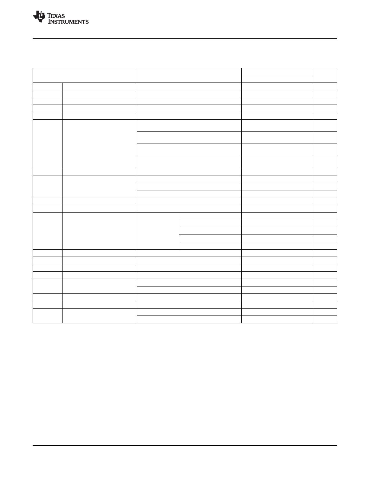
OUT1
OUT2
GND
6
5
4
EN1
IN
EN2
1
2
3
TLV710
TLV711
1.5mmx1.5mmSON-6
(TOPVIEW)
IN
EN1
EN2
GND
OUT1
OUT2
ON
OFF
ON
OFF
V
IN
C
IN
C
1 F
Ceramic
m
OUT1
C
OUT2
1 F
Ceramic
m
V
OUT1
V
OUT2
TLV710 Series
TLV711 Series
www.ti.com.cn
ZHCS452A –JULY 2010– REVISED AUGUST 2010
适合便携式设备的双通道、
200mA、低 I
Q
、 低 压 降 稳 压 器
1
特性 说明
2
• 超低的压降:
TLV710 和 TLV711 系列双通道、低压降 (LDO) 线性
稳压器是具有卓越的线路输入电压及负载瞬态响应性能
– 150mV(在 I
OUT
=200mA 和 V
OUT
= 2.8V 时)
的低静态电流器件。 这些 LDO 专门针对功耗敏感型应
– 75mV(在 I
OUT
=100mA 和 V
OUT
= 2.8V时)
用而设计。 这些器件在整个温度范围内提供了2% 的
– 40mV(在 I
OUT
=50mA 和 V
OUT
= 2.8V时)
典型准确度。
• 在整个温度范围内可提供 2% 的准确度
• 低I
Q
:每个稳压器为 35μA
TLV711系列提供了一种有源下拉电路,以对输出进行
• 可提供多种固定输出电压组合:1.2V至4.8V
快速放电。
• 高PSRR:70dB(在 1kHz 频率下)
此外,TLV711-D 器件系列还在 EN 引脚上布设了下拉
• 可在采用 0.1μF 的有效电容时保持稳定
(1)
电阻器。 这种设计有助于在信号驱动 EN 引脚处于一
• 过流和热保护
种微弱、不确定状态(例如:在启动期间有可能为三态
• 用于每个输出的专用 V
REF
最大限度地降低了串扰
的处理器 GPIO)时停用器件。 该下拉电阻器可将至
• 采用1.5mm x 1.5mm SON-6 封装
EN 引脚的电压拉低至 0V,从而停用器件。
(1)
请参见 应用信息部分中的 输入和输出电容器要求
TLV710 和 TLV711系列采用 1.5mm x 1.5mm SON-6
应用
封装,而且非常适合于手持式应用。
• 无线头戴式耳机、智能手机、PDA
• MP3 播放器及其他手持式产品
图 1. 典型应用电路
1
Please be aware that an important notice concerning availability, standard warranty, and use in critical applications of Texas
Instruments semiconductor products and disclaimers thereto appears at the end of this data sheet.
2All trademarks are the property of their respective owners.
PRODUCTION DATA information is current as of publication date.
Copyright © 2010, Texas Instruments Incorporated
Products conform to specifications per the terms of the Texas
Instruments standard warranty. Production processing does not English Data Sheet: SBVS142A
necessarily include testing of all parameters.


剩余33页未读,继续阅读


评论0