TI-TLV5580.pdf
需积分: 10 93 浏览量
2022-11-27
16:19:29
上传
评论 4
收藏 536KB PDF 举报

SLAS205B − DECEMBER 1998 − REVISED OCTOBER 2003
www.ti.com
D 8-Bit Resolution 80 MSPS Sampling
Analog-to-Digital Converter (ADC)
D Low Power Consumption: 165 mW Typ
Using External references
D Wide Analog Input Bandwidth: 700 MHz Typ
D 3.3 V Single-Supply Operation
D 3.3 V TTL/CMOS-Compatible Digital I/O
D Internal Bottom and Top Reference Voltages
D Adjustable Reference Input Range
D Power Down (Standby) Mode
D Separate Power Down for Internal Voltage
References
D Three-State Outputs
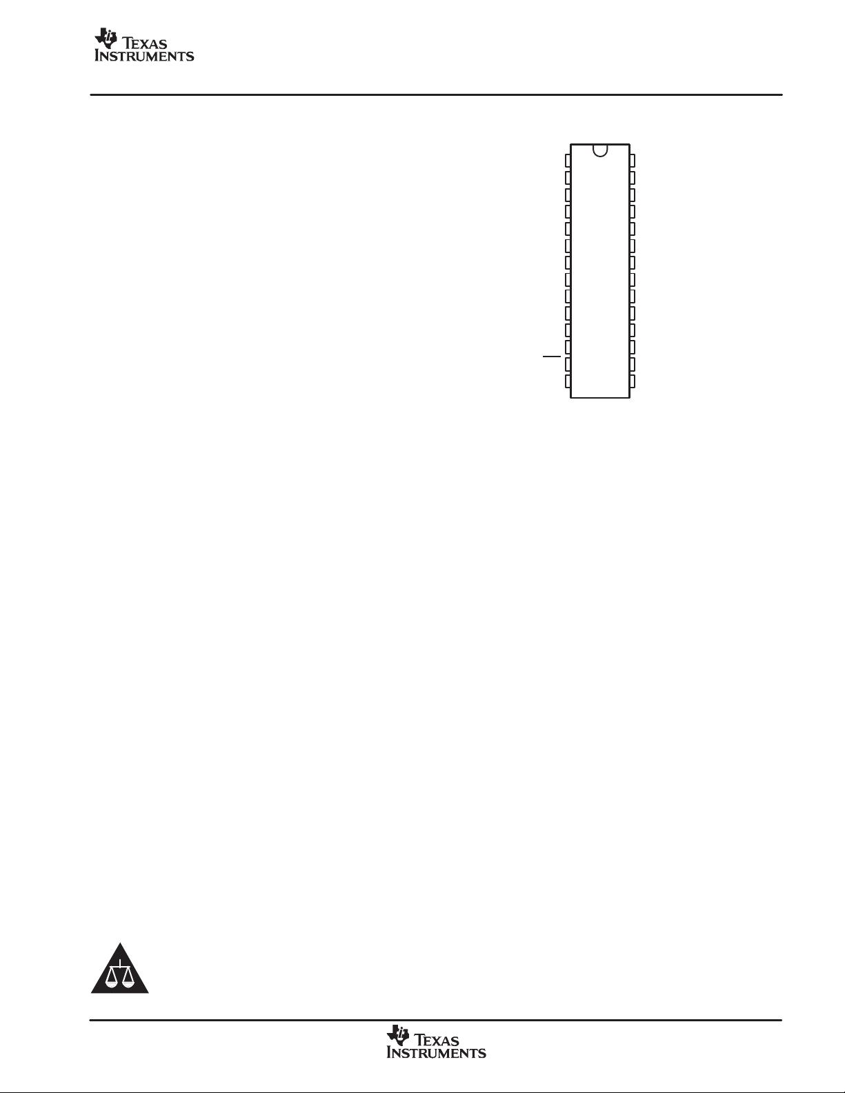
D 28-Pin Small Outline IC (SOIC) and Thin
Shrink SOP (TSSOP) Packages
D Applications
− Digital Communications
− Flat Panel Displays
− High-Speed DSP Front-End
(TMS320C6000)
− Medical Imaging
− Graphics Processing (Scan Rate/Format
Conversion)
− DVD Read Channel Digitization
DESCRIPTION
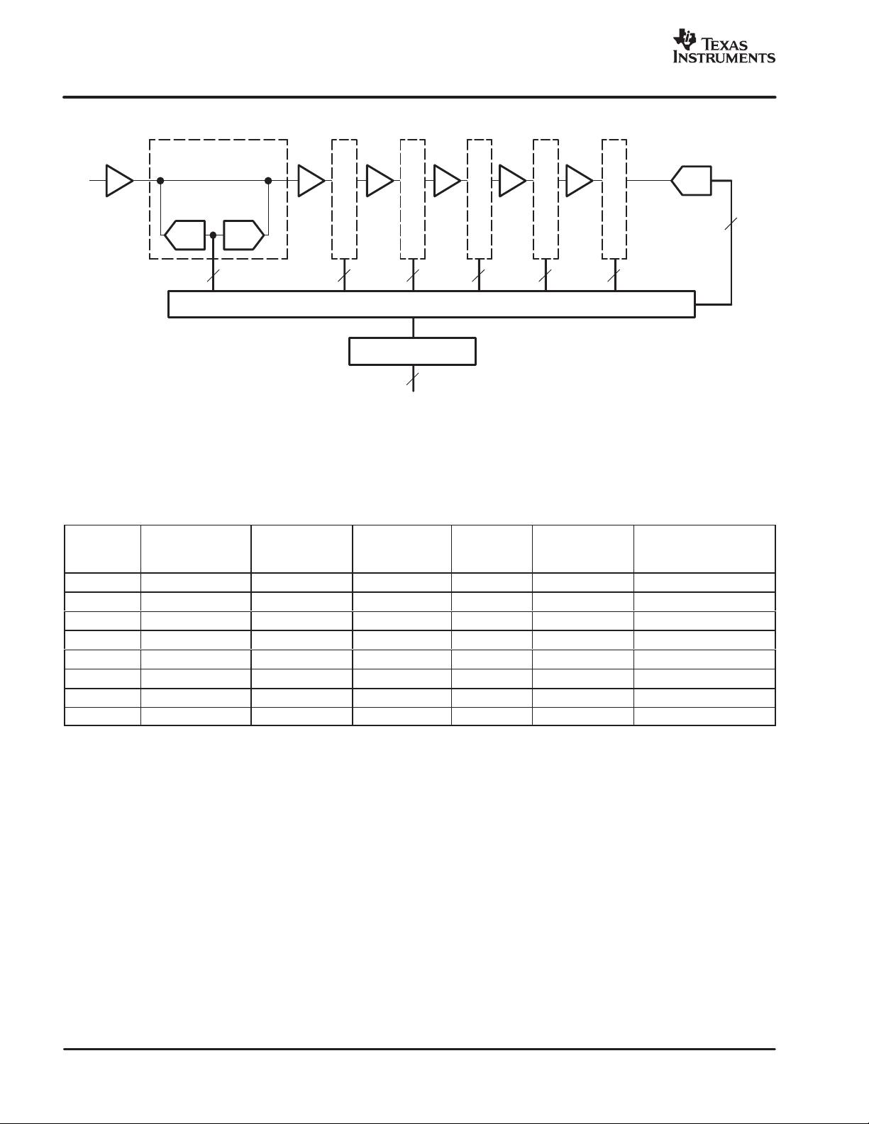
The TLV5580 is an 8-bit 80 MSPS high-speed A/D
converter. It converts the analog input signal into
8-bit binary-coded digital words up to a sampling
rate of 80 MHz. All digital inputs and outputs are
3.3 V TTL/CMOS-compatible.
The device consumes very little power due to the
3.3 V supply and an innovative single-pipeline
architecture implemented in a CMOS process.
The user obtains maximum flexibility by setting
both bottom and top voltage references from
user-supplied voltages. If no external references
are available, on-chip references are available for
internal and external use. The full-scale range is
1 Vpp up to 1.6 Vpp, depending on the analog
supply voltage. If external references are
available, the internal references can be disabled
independently from the rest of the chip, resulting
in an even greater power saving.
While usable in a wide variety of applications, the
device is specifically suited for the digitizing of
high-speed graphics and for interfacing to LCD
panels or LCD/DMD projection modules . Other
applications include DVD read channel
digitization, medical imaging and
communications. This device is suitable for IF
sampling of communication systems using
sub-Nyquist sampling methods because of its
high analog input bandwidth.
! "#$ ! %#&'" ($) (#"!
" !%$""! %$ *$ $! $+! !#$! !(( ,-)
(#" %"$!!. ($! $"$!!'- "'#($ $!. '' %$$!)
Please be aware that an important notice concerning availability, standard warranty, and use in critical applications of
Texas Instruments semiconductor products and disclaimers thereto appears at the end of this data sheet.
All trademarks are the property of their respective owners.
1
2
3
4
5
6
7
8
9
10
11
12
13
14
28
27
26
25
24
23
22
21
20
19
18
17
16
15
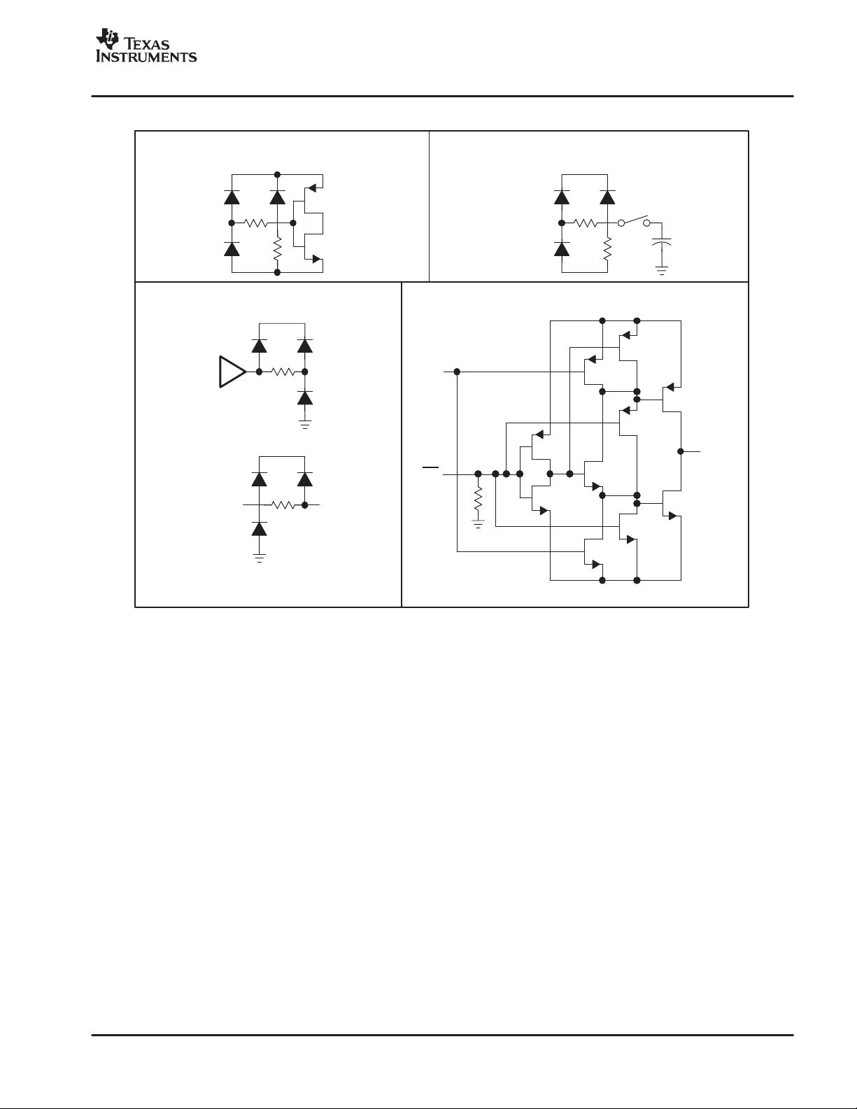
DRV
DD
D0
D1
D2
D3
D4
D5
D6
D7
DRV
SS
DV
SS
CLK
OE
DV
DD
AV
SS
AV
DD
AIN
CML
PWDN_REF
AV
SS
REFBO
REFBI
REFTI
REFTO
AV
SS
BG
AV
DD
STBY
DW OR PW PACKAGE
(TOP VIEW)
Copyright 1999−2003, Texas Instruments Incorporated
www.ti.com


剩余37页未读,继续阅读
资源评论


