TI-TMDS341.pdf
需积分: 10 146 浏览量
2023-02-07
23:05:16
上传
评论 4
收藏 1.71MB PDF 举报

www.ti.com
FEATURES
APPLICATIONS
DESCRIPTION
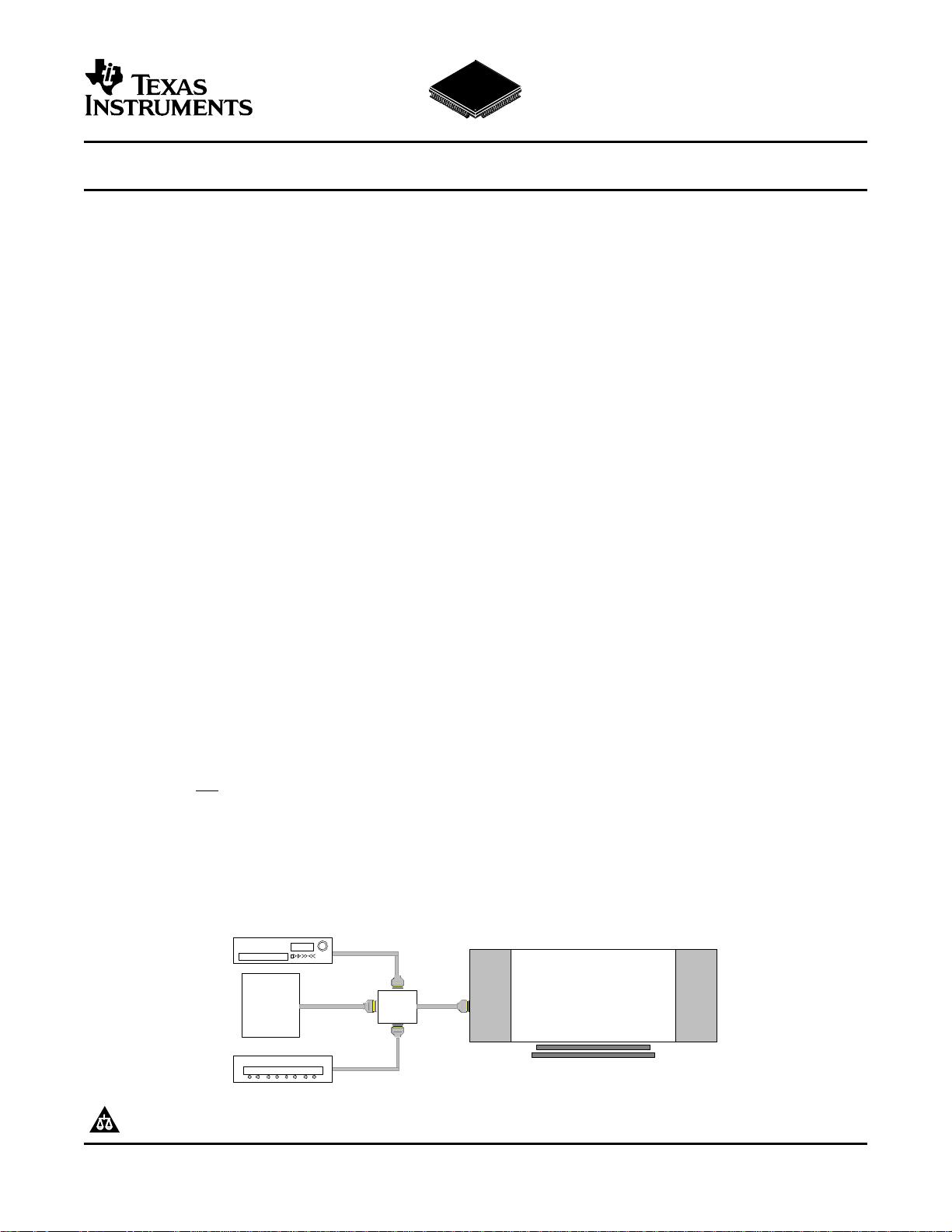
TYPICAL APPLICATION
PC
TMDS
341
DVD Player
STB
Digital TV
or
Game
Machine
TMDS341
SLLS660B – AUGUST 2005 – REVISED JANUARY 2006
3-TO-1 DVI/HDMI SWITCH
• HBM ESD Protection Exceeds 3 kV
• Designed for Signaling Rates up to 1.65 Gbps • 3.3-V Supply Operation
in Support of UXGA Display
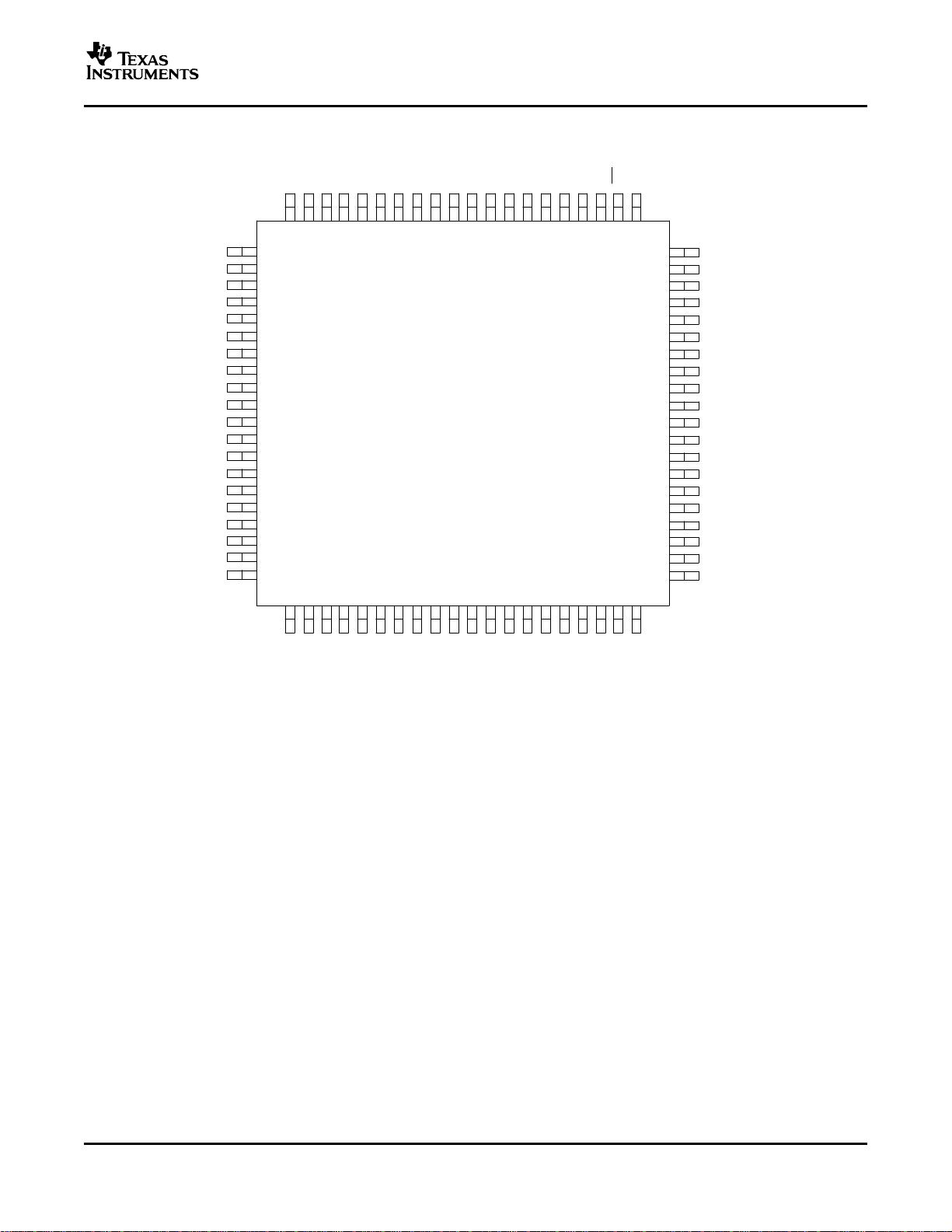
• 80-Pin TQFP Package
• Differential Interface Compatible with
• ROHS Compatible and 260 ° C Reflow Rated
Transition Minimized Differential Signaling
(TMDS) Electrical Specification
• Each Port Supports HDMI or DVI Inputs
• Switching From Three Digital-Video (DVI) or
Digital-Audio Visual (HDMI) Sources
• Isolated Digital Display Control (DDC) Bus for
• Digital TV
Unused Ports
• Digital Projector
• 5-V Tolerance to all DDC and HPD_SINK
• Audio Video Receiver
Inputs
• Integrated Receiver Termination
• Inter-Pair Output Skew < 100 ps
• 8-dB Receiver Equalization to Compensate for
5-m DVI Cable Losses
• High Impedance Outputs When Disabled
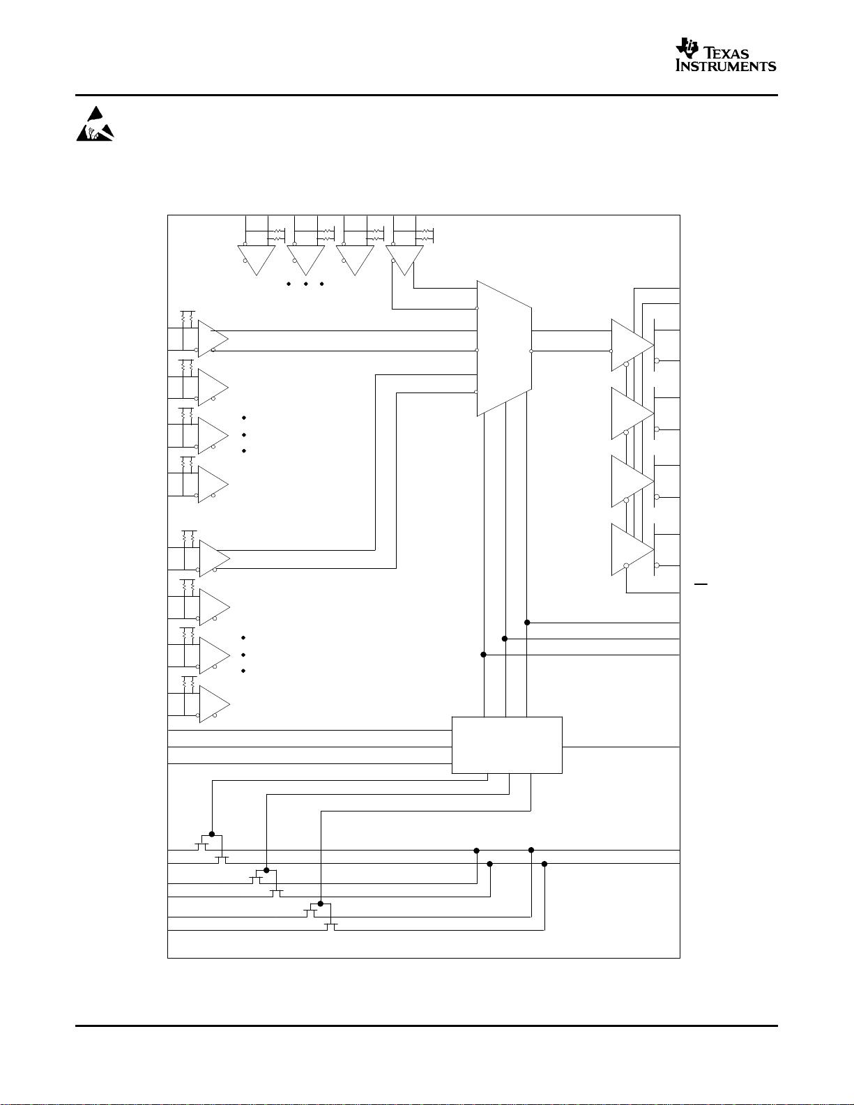
The TMDS341 is a 3-port digital video interface (DVI) or high-definition multimedia interface (HDMI) switch that
allows up to 3 DVI or HDMI ports to be switched to a single display terminal. Four TMDS channels, one hot plug
detector, and an I
2
C interface are supported on each port. Each TMDS channel allows signaling rates up to 1.65
Gbps.
The active source is selected by configuring source selectors, S1, S2, and S3. The selected TMDS inputs from
each port are switched through a 3-to-1 multiplexer. The I
2
C interface of the selected input port is linked to the
I
2
C interface of the output port, and the hot plug detector (HPD) of the selected input port is output to
HPD_SINK. For the unused ports, the I
2
C interfaces are isolated, and the HPD pins are kept low.
Termination resistors (50- Ω ), pulled up to V
CC
, are integrated at each receiver input pin. External terminations are
not required. A precision resistor is connected externally from the VSADJ pin to ground for setting the differential
output voltage to be compliant with the TMDS standard. When the output is connected to a standard TMDS
termination and OE is high, the output is high impedance.
The TMDS341 provides fixed 8-dB input equalization and selectable 3-dB output de-emphasis to optimize
system performance through 5-meter or longer DVI compliant cables. The device is characterized for operation
from 0 ° C to 70 ° C.
Please be aware that an important notice concerning availability, standard warranty, and use in critical applications of Texas
Instruments semiconductor products and disclaimers thereto appears at the end of this data sheet.
PRODUCTION DATA information is current as of publication date.
Copyright © 2005–2006, Texas Instruments Incorporated
Products conform to specifications per the terms of the Texas
Instruments standard warranty. Production processing does not
necessarily include testing of all parameters.
剩余24页未读,继续阅读
资源评论


