TI-TMDS181.pdf

需积分: 0 185 浏览量
更新于2023-02-07
收藏 2.83MB PDF 举报
**TI-TMDS181 HDMI重定时器**是德州仪器(Texas Instruments)推出的一款针对数字视频和音频传输的高性能芯片。这款芯片主要用于解决在HDMI传输过程中由于长距离或复杂环境导致的信号质量下降问题,它能有效地提高信号的稳定性和可靠性。
### 主要特性
1. **高速数据处理能力**:TMDS181支持高达6Gbps的数据速率,这意味着它可以处理4k2k60p的分辨率,即4096×2160像素的60帧每秒视频,同时支持16位色深或1080p更高刷新率的视频流。
2. **时钟和数据恢复(CDR)**:内置的CDR电路确保了HDMI输入端口和输出端口之间的时钟同步,有效补偿随机抖动,保持信号的精确传输。
3. **自适应均衡器**:TMDS181拥有自适应接收器均衡器,可以根据输入信号的品质动态调整,或使用可编程的固定均衡器,以适应不同长度和质量的电缆或PCB线路。
4. **I2C和引脚编程**:用户可以通过I2C总线或引脚设置进行配置,方便地调整设备的工作状态和性能。
5. **5+ 位对内偏移补偿**:这种补偿功能可以校正信号的幅度差异,确保信号的准确无误。
6. **ARC支持**:支持音频返回通道(ARC),允许音频信号双向传输,例如从电视到音频接收器。
7. **链路调试工具**:内置的眼图分析功能可以在接收均衡器后查看信号质量,帮助调试和优化链接性能。
8. **温度范围**:提供扩展商业温度范围(0°C 至 85°C)和工业温度范围(-40°C 至 85°C)的产品型号,以适应各种工作环境。
### 应用场景
- **数字电视**:用于提升电视接收的视频和音频质量。
- **数字投影仪**:增强投影仪的图像稳定性。
- **音频/视频设备**:如蓝光DVD播放器,确保音视频同步传输。
- **监视器**:提高显示器的图像清晰度和色彩准确性。
- **台式机/一体化计算机**:改善电脑的显示输出质量。
- **有源线缆**:在长距离HDMI线缆中提高信号完整性。
### 工作原理
TMDS181在数据速率低于1.0Gbps时作为重驱动器工作,支持HDMI 1.4b标准;而在高于此速率时,自动转换为重定时器模式,符合HDMI 2.0a标准。双电源轨设计(VDD 1.2V和VCC 3.3V)有助于降低功耗。此外,该器件具备多种电源管理策略,进一步减少了整体功耗。
总结来说,TMDS181是一款高效、灵活的HDMI重定时器,适用于各种需要高质量音视频传输的场合,通过其先进的信号处理技术,确保了在复杂环境中也能保持良好的信号质量和稳定性。
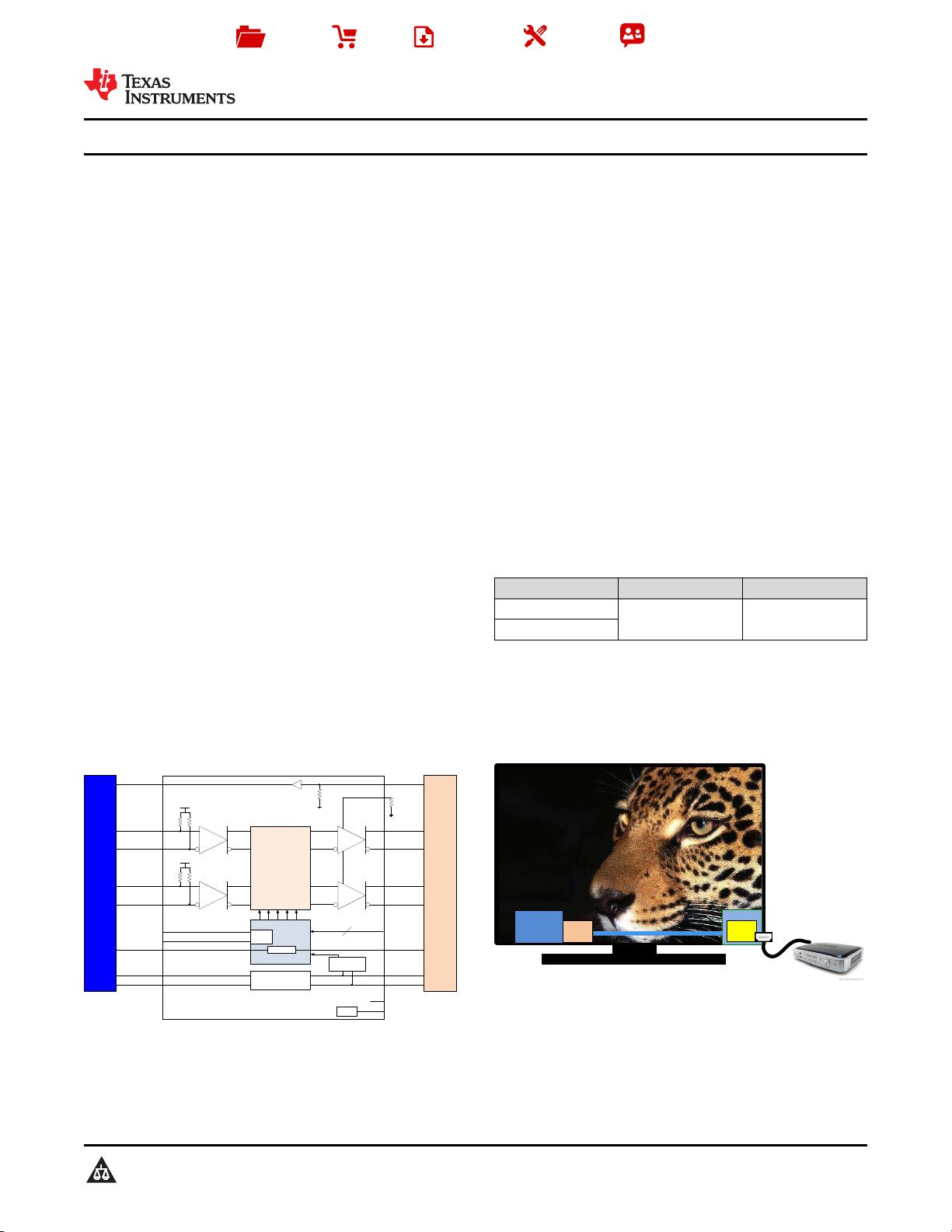
IN_CLKp
IN_CLKn
IN_D[2:0]p
IN_D[2:0]n
50Q
50Q50Q
50Q
Data Registers
SWAP
PLL
PLL Control
SERDES
Polarity
VBIAS
VBIAS
OUT_CLKp
OUT_D[2:0]p
OUT_CLKn
OUT_D[2:0]n
EQ
EQ
SDA_CTL
SCL_CTL
VSADJ
TMDS
TMDS
ACTIVE DDC BLOCK
HPD_SNK
HPD_SRC
190<Q
SDA_SRC
SCL_SRC
SDA_SNK
SCL_SNK
SPDIF_IN
ARC_OUT
GND
VDD
VCC
1.2V
3.3V
VREG
GPU
HDMI
Conn
7.06 lQ
Control
6
DDC Snoop
Block
Control Block, I2C
Registers,
DDC. ARC
Local I2C
Control
ARC
Copyright © 2016, Texas Instruments Incorporated
Interface
Unit
Digital TV
Audiovisual
Processing
Unit
HDMI
SW/HD
TMDS
181
Product
Folder
Order
Now
Technical
Documents
Tools &
Software
Support &
Community
An IMPORTANT NOTICE at the end of this data sheet addresses availability, warranty, changes, use in safety-critical applications,
intellectual property matters and other important disclaimers. PRODUCTION DATA.
English Data Sheet: SLASE75
TMDS181, TMDS181I
ZHCSE70D –AUGUST 2015–REVISED SEPTEMBER 2017
TMDS181x 6Gbps TMDS 重重定定时时器器
1
1 特特性性
1
• HDMI™ 输入端口与输出端口间具有时钟和数据恢
复 (CDR) 电路,支持高达 6Gbps 的数据速率
• 在重定时器模式下可兼容高达 6Gbps 的 HDMI™
电气参数
• 支持 4k2k60p 和高达 WUXGA 16 位色深或
1080p,具有更高的刷新率
• 对输入流重新定时以补偿随机抖动
• 自适应接收器均衡器或可编程固定均衡器
• I
2
C 和引脚设置可编程
• 5+ 位对内偏移补偿
• 支持单端模式 ARC
• 链路调试工具包括位于RX 均衡器之后眼图
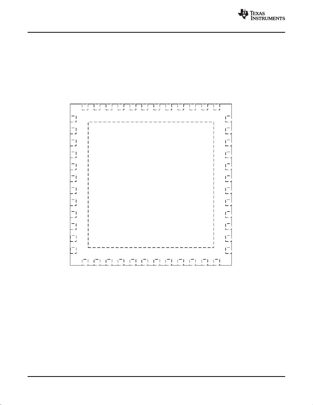
• 48 引脚 7mm × 7mm 0.5mm 间距超薄型四方扁平
无引线 (VQFN) 封装
• 扩展商业温度范围为 0°C 至 85°C (TMDS181)
• 工业温度范围为 -40°C 至 85°C (TMDS181I)
2 应应用用
• 数字电视
• 数字投影仪
• 音频/视频设备
• Blu-Ray™DVD
• 监视器
• 台式机/一体化计算机
• 有源线缆
3 说说明明
TMDS181x 是一款数字视频接口 (DVI) 或高清多媒体
接口 (HDMI™) 重定时器。TMDS181x 支持四条
TMDS 通道,音频返回通道 (SPDIF_IN/ARC_OUT) 和
数字显示控制 (DDC) 接口。TMDS181x 支持高达
6Gbps 的信号传输速率,可实现最高分辨率达
4k2k60p 24 位/像素和高达 WUXGA 16 位色深或
1080p,并且具有较高的刷新率。TMDS181x 经配置
可支持 HDMI2.0a 标准。TMDS181x 在低于 1.0Gbps
的数据速率下会自动配置为重驱动器,而在高于该速率
时会自动配置为重定时器。重驱动器模式支持
HDMI1.4b,数据速率高达 3.4Gbps
TMDS181x 支持双电源轨(V
DD
为 1.2V,V
CC
为
3.3V),有助于降低功耗。该器件采用多种电源管理
方法来降低整体功耗。TMDS181x 通过 I
2
C 或引脚设
置支持固定的接收 EQ 增益或自适应接收 EQ 控制,
以补偿不同长度的输入电缆或电路板走线。
器器件件信信息息
(1)
器器件件型型号号 封封装装 封封装装尺尺寸寸((标标称称值值))
TMDS181
VQFN (48) 7.00mm × 7.00mm
TMDS181I
(1) 如需了解所有可用封装,请参阅产品说明书末尾的可订购产品
附录。
空白
简简化化电电路路原原理理图图


剩余58页未读,继续阅读
124 浏览量
2023-02-07 上传
2023-02-07 上传
2023-02-07 上传
133 浏览量
2023-02-07 上传
2023-02-07 上传
2023-02-07 上传
121 浏览量
102 浏览量
2023-02-07 上传
资源评论


不觉明了
- 粉丝: 6255
- 资源: 5764


最新资源
- 毕设和企业适用springboot企业知识管理平台类及在线音乐平台源码+论文+视频.zip
- 毕设和企业适用springboot企业知识管理平台类及智慧社区管理平台源码+论文+视频.zip
- 毕设和企业适用springboot人才招聘类及企业资源规划平台源码+论文+视频.zip
- 毕设和企业适用springboot人才招聘类及社区服务平台源码+论文+视频.zip
- 毕设和企业适用springboot人才招聘类及食品配送管理平台源码+论文+视频.zip
- 毕设和企业适用springboot企业资源规划类及AI数据标注平台源码+论文+视频.zip
- 毕设和企业适用springboot企业资源规划类及车载智能管理平台源码+论文+视频.zip
- 毕设和企业适用springboot企业资源规划类及大数据实时处理系统源码+论文+视频.zip
- 毕设和企业适用springboot人才招聘类及视频内容管理平台源码+论文+视频.zip
- 毕设和企业适用springboot汽车管理类及网络营销平台源码+论文+视频.zip
- 毕设和企业适用springboot汽车管理类及物流信息平台源码+论文+视频.zip
- 毕设和企业适用springboot汽车管理类及销售管理平台源码+论文+视频.zip
- 毕设和企业适用springboot汽车管理类及物流追踪系统源码+论文+视频.zip
- 毕设和企业适用springboot汽车管理类及消费品管理平台源码+论文+视频.zip
- 毕设和企业适用springboot企业资源规划类及个性化广告平台源码+论文+视频.zip
- 毕设和企业适用springboot企业资源规划类及教育评价系统源码+论文+视频.zip
