没有合适的资源?快使用搜索试试~ 我知道了~
TI-TMDS351.pdf
需积分: 9 0 下载量 67 浏览量
2023-02-07
23:04:57
上传
评论 4
收藏 587KB PDF 举报
温馨提示
试读
27页
HDMI开关
资源推荐
资源详情
资源评论
STB
DigitalTV
DVDPlayer
Game
Console
TMDS351
3-to-1
PHY SX
TMDS351
www.ti.com
SLLS840B –MAY 2007– REVISED JULY 2011
2.5 Gbps 3-TO-1 DVI/HDMI SWITCH
Check for Samples: TMDS351
• 3.3-V Fixed Supply to TMDS I/Os
1
FEATURES
• 5-V Fixed Supply to HPD, DDC, and Source
• Compatible with HDMI 1.3a
Selection Circuits
• Supports 2.5 Gbps Signaling Rate for 480i/p,
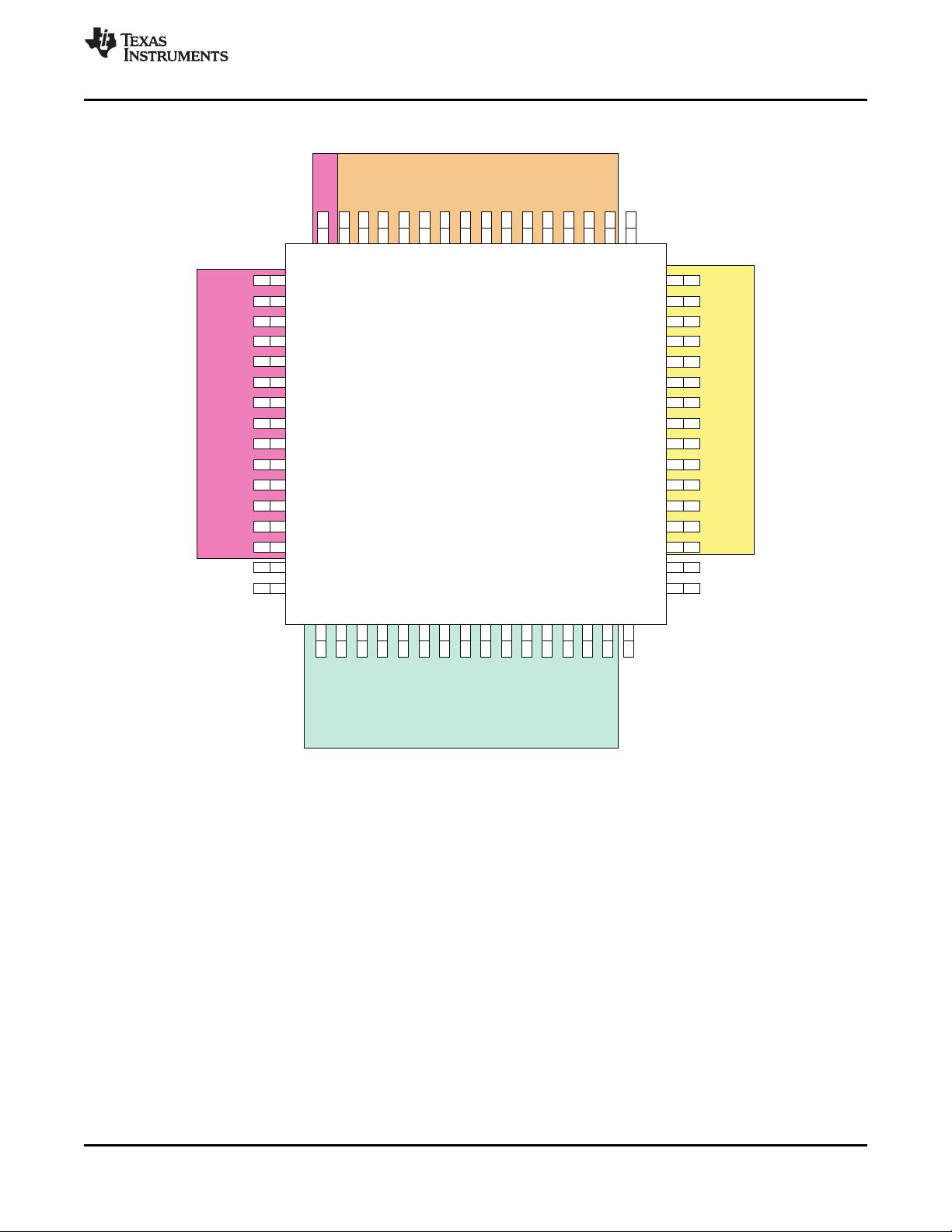
• 64-Pin TQFP Package
720i/p, and 1080i/p Resolutions up to 12-Bit
• ROHS Compatible and 260°C Reflow Rated
Color Depth
• Integrated Receiver Termination
APPLICATIONS
• Selectable Receiver Equalization to
Accommodate to Different Input Cable
• Digital TV
Lengths
• Digital Projector
• Intra-Pair Skew < 40 ps
• Inter-Pair Skew < 65 ps
• HBM ESD Protection Exceeds 8 kV to TMDS
Inputs
DESCRIPTION
The TMDS351 is a 3-port digital video interface (DVI) or high-definition multimedia interface (HDMI) switch that
allows up to 3 DVI or HDMI ports to be switched to a single display terminal. Four TMDS channels, one hot plug
detector, and a digital display control (DDC) interface are supported on each port. Each TMDS channel supports
signaling rates up to 2.5 Gbps to allow 1080p resolution in 12-bit color depth.
When S1 is high and S2 is low, all input terminations are disconnected, TMDS inputs are high impedance with
standard TMDS terminations, all internal MOSFETs are turned off to disable the DDC links, and all HPD outputs
are connected to the HPD_SINK. This allows the initiation of the HDMI physical address discovery process.
Termination resistors (50-Ω), pulled up to V
CC
, are integrated at each TMDS receiver input. External terminations
are not required. A precision resistor is connected externally from the VSADJ pin to ground for setting the
differential output voltage to be compliant with the TMDS standard.
The TMDS351 provides two levels of receiver input equalization for different ranges of cable lengths. Each
TMDS receiver owns frequency responsive equalization circuits. When EQ sets low, the receiver supports the
input connection in short range HDMI cables. When EQ sets high, the receiver supports the input connection in
long range HDMI cables. The TMDS351 supports power saving operation. When a system is under standby
mode and there is no digital audio/visual content from a connected source, the 3.3-V supply voltage, V
CC
, can be
powered off to minimize power consumption from the TMDS inputs, outputs, and internal switching circuits. The
HPD, DDC, and source selection circuits are powered up by the 5-V supply voltage, V
DD
, to maintain the system
hot plug detect response, the DDC link from the selected source to the sink under system standby operation. The
device is characterized for operation from 0°C to 70°C.
Typical Application
1
Please be aware that an important notice concerning availability, standard warranty, and use in critical applications of Texas
Instruments semiconductor products and disclaimers thereto appears at the end of this data sheet.
PRODUCTION DATA information is current as of publication date.
Copyright © 2007–2011, Texas Instruments Incorporated
Products conform to specifications per the terms of the Texas
Instruments standard warranty. Production processing does not
necessarily include testing of all parameters.
SCL_SINK
SDA_SINK
HPD_SINK
S1
S2
.
.
.
.
.
.
.
.
.
Control
Logic
Y4
Z4
VSADJ
TMDS
Driver
TMDS
Driver
TMDS
Driver
TMDS
Driver
EQ
V
DD
Vcc
R
INT
TMDS
Rx
R
INT
Vcc
R
INT
TMDS
Rx
R
INT
Vcc
R
INT
TMDS
Rx
R
INT
Vcc
R
INT
TMDS
Rx
R
INT
Vcc
R
INT
TMDS
Rx
R
INT
Vcc
R
INT
TMDS
Rx
R
INT
Vcc
R
INT
TMDS
Rx
R
INT
Vcc
R
INT
TMDS
Rx
R
INT
Vcc
R
INT
TMDS
Rx
R
INT
Vcc
R
INT
TMDS
Rx
R
INT
Vcc
R
INT
TMDS
Rx
R
INT
Vcc
R
INT
TMDS
Rx
R
INT
B11
A11
B12
A12
B13
A13
B14
A14
A24
B24
A23
B23
A22
B22
A21
B21
A34
B34
A33
B33
A32
B32
A31
B31
HPD1
HPD2
HPD3
SCL1
SDA1
SCL2
SDA2
SCL3
SDA3
Y3
Z3
Y1
Z1
Y2
Z2
HPD/DDC
PowerSupply
TMDS351
SLLS840B –MAY 2007– REVISED JULY 2011
www.ti.com
These devices have limited built-in ESD protection. The leads should be shorted together or the device placed in conductive foam
during storage or handling to prevent electrostatic damage to the MOS gates.
FUNCTIONAL BLOCK DIAGRAM
2 Copyright © 2007–2011, Texas Instruments Incorporated
1
2
3
4
5
6
7
8
9
10
11
12
13
14
15
16
TMDS351
64-pin TQFP
SDA3
SCL3
GND
B31
A31
Vcc
B32
A32
GND
B33
A33
Vcc
B34
A34
GND
VSADJ
17
18
19
20
21
22
23
24
25
26
27
28
29
30
31
32
Y4
Z4
Vcc
Y3
Z3
GND
Y2
Z2
Vcc
Y1
Z1
GND
SCL_SINK
SDA_SINK
HPD_SINK
S1
48
47
46
45
44
43
42
41
40
39
38
37
36
35
34
33
A14
B14
Vcc
A13
B13
GND
A12
B12
Vcc
A11
B11
SCL1
SDA1
HPD1
EQ
S2
64
63
62
61
60
59
58
57
56
55
54
53
52
51
50
49
HPD3
A24
B24
Vcc
A23
B23
GND
A22
B22
Vcc
A21
B21
SCL2
SDA2
HPD2
VDD
TMDS351
www.ti.com
SLLS840B –MAY 2007– REVISED JULY 2011
PAG PACKAGE
(TOP VIEW)
Copyright © 2007–2011, Texas Instruments Incorporated 3
TMDS351
SLLS840B –MAY 2007– REVISED JULY 2011
www.ti.com
PIN FUNCTIONS
PIN
I/O DESCRIPTION
NAME NO.
A11, A12, A13, A14 39, 42, 45, 48 I Source port 1 TMDS positive inputs
A21, A22, A23, A24 54, 57, 60, 63 I Source port 2 TMDS positive inputs
A31, A32, A33, A34 5, 8, 11, 14 I Source port 3 TMDS positive inputs
B11, B12, B13, B14 38, 41, 44, 47 I Source port 1 TMDS negative inputs
B21, B22, B23, B24 53, 56, 59, 62 I Source port 2 TMDS negative inputs
B31, B32, B33, B34 4, 7, 10, 13 I Source port 3 TMDS negative inputs
3, 9, 15, 22, 28,
GND Ground
43, 58
TMDS Input equalization selector (control pin)
EQ 34 I EQ = Low – HDMI 1.3 compliant cable
EQ = High – 10m 28 AWG HDMI cable
HPD1 35 O Source port 1 hot plug detector output (status pin)
HPD2 50 O Source port 2 hot plug detector output (status pin)
HPD3 64 O Source port 3 hot plug detector output (status pin)
HPD_SINK 31 I Sink port hot plug detector input (status pin)
SCL1 37 I/O Source port 1 DDC I
2
C clock line
SCL2 52 I/O Source port 2 DDC I
2
C clock line
SCL3 2 I/O Source port 3 DDC I
2
C clock line
SCL_SINK 29 I/O Sink port DDC I
2
C clock line
SDA1 36 I/O Source port 1 DDC I
2
C data line
SDA2 51 I/O Source port 2 DDC I
2
C data line
SDA3 1 I/O Source port 3 DDC I
2
C data line
SDA_SINK 30 I/O Sink port DDC I
2
C data line
S1, S2 32. 33 I Source selector
6, 12, 19, 25, 40,
V
CC
Power supply
46, 55, 61
V
DD
49 HPD/DDC Power supply
VSADJ 16 I TMDS compliant voltage swing control (control pin)
Y1, Y2, Y3, Y4 26,23,20,17 O Sink port TMDS positive outputs
Z1, Z2, Z3, Z4 27,24,21,18 O Sink port TMDS negative outputs
4 Copyright © 2007–2011, Texas Instruments Incorporated
TMDS351
www.ti.com
SLLS840B –MAY 2007– REVISED JULY 2011
Table 1. Source Selection Lookup
(1)
CONTROL PINS I/O SELECTED HOT PLUG DETECT STATUS
SCL_SINK
S2 S1 Y/Z HPD1 HPD2 HPD3
SDA_SINK
A1/B1
Terminations of A2/B2 SCL1
H H HPD_SINK L L
and A3/B3 are SDA1
disconnected
A2/B2
Terminations of A1/B1 SCL2
H L L HPD_SINK L
and A3/B3 are SDA2
disconnected
A3/B3
Terminations of A1/B1 SCL3
L L L L HPD_SINK
and A2/B2 are SDA3
disconnected
None (Z)
None (Z)
Are pulled HIGH by
L H All terminations are HPD_SINK HPD_SINK HPD_SINK
external pull-up
disconnected
termination
(1) H: Logic high; L: Logic low; X: Don't care; Z: High impedance
Copyright © 2007–2011, Texas Instruments Incorporated 5
剩余26页未读,继续阅读
资源评论
不觉明了
- 粉丝: 3152
- 资源: 5416
上传资源 快速赚钱
- 我的内容管理 展开
- 我的资源 快来上传第一个资源
- 我的收益 登录查看自己的收益
- 我的积分 登录查看自己的积分
- 我的C币 登录后查看C币余额
- 我的收藏
- 我的下载
- 下载帮助
安全验证
文档复制为VIP权益,开通VIP直接复制
信息提交成功