TI-TMDS251.pdf
需积分: 10 113 浏览量
2023-02-07
23:05:34
上传
评论 4
收藏 593KB PDF 举报

STB
DigitalTVDVDPlayer
TMDS251
2-to-1
PHY SX
TMDS251
www.ti.com
SLLS852A –AUGUST 2007– REVISED JULY 2011
2.5 Gbps 2-TO-1 DVI/HDMI SWITCH
Check for Samples: TMDS251
• 3.3-V Fixed Supply to TMDS I/Os
1
FEATURES
• 5-V Fixed Supply to HPD, DDC, and Source
• Compatible with HDMI 1.3a
Selection Circuits
• Supports 2.5 Gbps Signaling Rate for 480i/p,
• 64-Pin TQFP Package
720i/p, and 1080i/p Resolutions up to 12-Bit
• Footprint Compatible with 3-to-1 Switch
Color Depth
TMDS351 with Port 3 Disabled
• Integrated Switchable Receiver Termination
• ROHS Compatible and 260°C Reflow Rated
• Selectable Receiver Equalization to
• TMDS250 is Available with Port 1 Disabled and
Accommodate to Different Input Cable
Ports 2 and 3 Enabled
Lengths
• Supports 5-V to 3.3-V Level Shifting on DDC
• Intra-Pair Skew < 40 ps
Links
• Inter-Pair Skew < 65 ps
• HBM ESD Protection Exceeds 8 kV to TMDS
APPLICATIONS
Inputs
• Digital TV
• Digital Projector
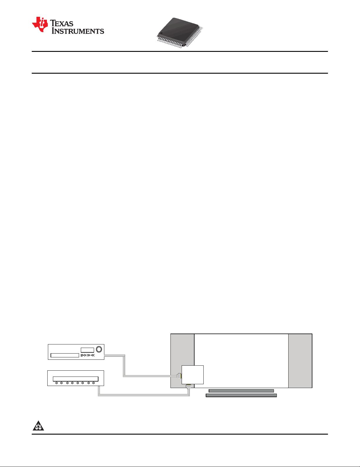
DESCRIPTION
The TMDS251 is a 2-port digital video interface (DVI) or high-definition multimedia interface (HDMI) switch that
allows up to 2 DVI or HDMI ports to be switched to a single display terminal. Four TMDS channels, one hot plug
detector, and a digital display control (DDC) interface are supported on each port. Each TMDS channel supports
signaling rates up to 2.5 Gbps to allow 1080p resolution in 12-bit color depth.
The input port is enabled by configuring source selectors, S1 and S2. When an input port is selected, the TMDS
inputs are connected to the TMDS outputs through a 2-to-1 multiplexer, the MOSFET between the input DDC
channel and the output DDC channel is turned on, and the HPD output follows the state of the HPD_SINK. The
other input port is inactive with disconnected input terminations, disconnected TMDS inputs to the outputs,
disconnected DDC inputs to the outputs, and the HPD outputs are low state. Check the source selection look up
table for the details of port selections.
When S1 is high and S2 is low, all input terminations are disconnected, TMDS inputs are high impedance with
standard TMDS terminations, all internal MOSFETs are turned off to disable the DDC links, and all HPD outputs
are connected to the HPD_SINK. This allows the initiation of the HDMI physical address discovery process.
Termination resistors (50-Ω), pulled up to V
CC
, are integrated at each TMDS receiver input. External terminations
are not required. A precision resistor is connected externally from the VSADJ pin to ground for setting the
differential output voltage to be compliant with the TMDS standard.
Typical Application
1
Please be aware that an important notice concerning availability, standard warranty, and use in critical applications of Texas
Instruments semiconductor products and disclaimers thereto appears at the end of this data sheet.
PRODUCTION DATA information is current as of publication date.
Copyright © 2007–2011, Texas Instruments Incorporated
Products conform to specifications per the terms of the Texas
Instruments standard warranty. Production processing does not
necessarily include testing of all parameters.


剩余25页未读,继续阅读
资源评论


