没有合适的资源?快使用搜索试试~ 我知道了~
TI-LMK03806.pdf
需积分: 12 0 下载量 74 浏览量
2022-11-30
12:56:57
上传
评论 4
收藏 1.87MB PDF 举报
温馨提示
试读
68页
TI-LMK03806.pdf
资源推荐
资源详情
资源评论
OSCin
Divide
Divide
OSCout1
OSCout0
CLKout6
CLKout7
CLKout8
CLKout9
CLKout10
CLKout11
CLKout0
CLKout1
CLKout2
CLKout3
CLKout4
CLKout5
Divide
Divide
Divide
Divide
Divide
PLL
Product
Folder
Order
Now
Technical
Documents
Tools &
Software
Support &
Community
An IMPORTANT NOTICE at the end of this data sheet addresses availability, warranty, changes, use in safety-critical applications,
intellectual property matters and other important disclaimers. PRODUCTION DATA.
English Data Sheet: SNAS522
LMK03806
ZHCSHU9J –SEPTEMBER 2011–REVISED MARCH 2018
具具有有 14 个个可可编编程程输输出出的的 LMK03806 超超低低抖抖动动时时钟钟发发生生器器
1
1 特特性性
1
• 高性能、超低抖动时钟发生器
• 低抖动
– 输出频率为 312.5MHz 时抖动小于 50fs
(1.875MHz – 20MHz)
– 输出频率为 312.5MHz 时抖动小于 150fs
(12kHz – 20MHz)
• 从低成本晶体或外部时钟生成多个时钟。
• 14 路可编程输出格式(LVDS、LVPECL、
CMOS)的输出
• 多达 8 个独特输出频率。
• 工业温度范围:–40°C 至 85°C
• 2.37GHz – 2.6GHz 的可调 VCO 频率
• 可编程分频器从低成本晶体生成多个时钟。
• 3.15V 至 3.45V 工作电压
2 应应用用
• SONET/SDH 中的超高速串行接口
• 千兆位级以太网和光纤通道线卡
• 用于 RAN 的基带单元 (BBU) 应用
• GPON OLT/ONU、高速串行接口(如 PCIe、
XAUI、SATA、SAS)
• 时钟 ADC 和 DAC
• 时钟 DSP、微处理器和 FPGA
3 说说明明
LMK03806 器件是一款高性能、超低抖动、多速率时
钟发生器,能够在频率高达 2.6GHz 的条件下针对 14
路输出合成 8 个不同的频率。每个输出时钟可设定为
LVDS、LVPECL 或 LVCMOS 格式。LMK03806 集成
了高性能的整数 N PLL、低噪声 VCO 和可编程输出分
频器,能够以低成本的晶体为 SONET、以太网、光纤
通道、XAUI、背板、PCIe、SATA 和网络处理器生成
多个参考时钟。
器器件件信信息息
(1)
器器件件型型号号 封封装装 封封装装尺尺寸寸((标标称称值值))
LMK03806 WQFN (64) 9.00mm x 9.00mm
(1) 如需了解所有可用封装,请参阅数据表末尾的可订购产品附
录。
功功能能方方框框图图
2
LMK03806
ZHCSHU9J –SEPTEMBER 2011–REVISED MARCH 2018
www.ti.com.cn
Copyright © 2011–2018, Texas Instruments Incorporated
目目录录
1 特特性性.......................................................................... 1
2 应应用用.......................................................................... 1
3 说说明明.......................................................................... 1
4 修修订订历历史史记记录录 ........................................................... 2
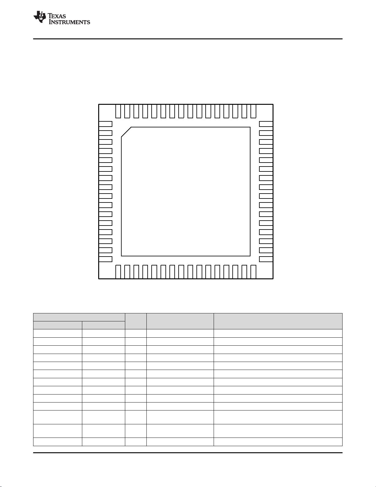
5 Pin Configuration and Functions......................... 3
6 Specifications......................................................... 5
6.1 Absolute Maximum Ratings ..................................... 5
6.2 ESD Ratings.............................................................. 5
6.3 Recommended Operating Conditions....................... 5
6.4 Thermal Information.................................................. 6
6.5 Electrical Characteristics........................................... 6
6.6 Timing Requirements.............................................. 14
6.7 Typical Characteristics............................................ 15
7 Parameter Measurement Information ................ 16
7.1 Differential Voltage Measurement Terminology ..... 16
8 Detailed Description............................................ 17
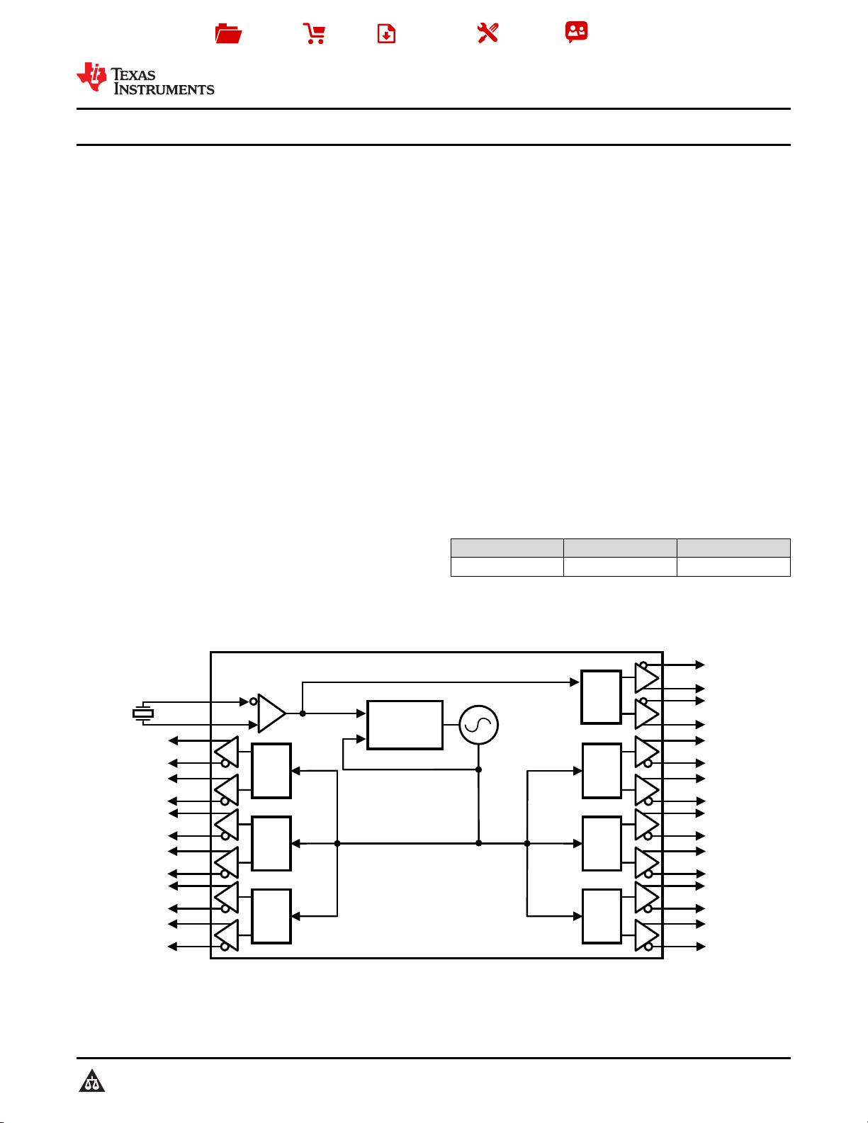
8.1 Overview ................................................................. 17
8.2 Functional Block Diagrams .................................... 17
8.3 Features Description............................................... 19
8.4 Device Functional Modes........................................ 21
8.5 Programming........................................................... 22
8.6 Register Maps......................................................... 23
9 Application and Implementation ........................ 43
9.1 Application Information............................................ 43
9.2 Typical Application ................................................. 49
9.3 System Examples ................................................... 55
9.4 Do's and Don'ts....................................................... 56
10 Power Supply Recommendations ..................... 56
10.1 Current Consumption and Power Dissipation
Calculations.............................................................. 56
11 Layout................................................................... 58
11.1 Layout Guidelines ................................................. 58
11.2 Layout Example .................................................... 59
12 器器件件和和文文档档支支持持 ..................................................... 60
12.1 器件支持................................................................ 60
12.2 文档支持................................................................ 60
12.3 相关链接................................................................ 60
12.4 社区资源................................................................ 60
12.5 商标 ....................................................................... 60
12.6 静电放电警告......................................................... 60
12.7 Glossary................................................................ 60
13 机机械械、、封封装装和和可可订订购购信信息息....................................... 60
4 修修订订历历史史记记录录
注:之前版本的页码可能与当前版本有所不同。
Changes from Revision I (November 2015) to Revision J Page
• Removed unresolvable cross-references. .............................................................................................................................. 6
• Added initial programming requirement of R3...................................................................................................................... 22
• Changed readback text from "rising" to "falling"................................................................................................................... 23
• Bolded pin 30 of register R3 for emphasis. .......................................................................................................................... 23
• Added table note to Default Device Register Settings After Power On Reset to clarify proper use of CLKout6................. 26
• Added note to Register R0 TO R5 regarding programming R3. .......................................................................................... 28
Changes from Revision H (August 2012) to Revision I Page
• 添加
器件信息
表、ESD
额定值
表、
热性能信息
表、
特性 说明
部分、
器件功能模式
、
应用和实施
部分、
电源建议
部
分、
布局
部分、
器件和文档支持
部分以及
机械、封装和可订购信息
部分。 ......................................................................... 1
• Separated Timing Requirements into its own section .......................................................................................................... 14
• Moved Serial MICROWIRE Timing Diagram and Terminology section ............................................................................... 19
• Moved Achievable Frequencies table and Common Frequency Plans table to Device Functional Modes section............. 21
• Added Driving OSCin Pins with a Differential Source section.............................................................................................. 44
• Added Frequency Planning with the LMK03806 and Configuring the PLL sections............................................................ 45
• Moved Thermal Management section and renamed it to Layout Guidelines....................................................................... 58
6364 62 61 60 59 58 57 56 55 54 53
CLKout8
CLKout9
CLKout10*
GPout0
CLKout8*
CLKout9*
Vcc12
CLKout10
CLKout11*
CLKout11
GPout1
Vcc13
DAP
52 51 50 49
CLKout6*
Vcc11
CLKout7*
CLKout7
OSCout1*
Vcc2
Vcc3
CLKout4
Vcc4
CLKout4*
CLKout5*
CLKout5
GND
NC
NC
Readback
NC
NC
Vcc5
OSCout1
38
37
39
40
41
42
43
44
45
46
47
48
Vcc7
CPout
Vcc9
CLKuWire
OSCin*
OSCout0
OSCout0*
Vcc8
LEuWire
DATAuWire
Vcc10
CLKout6
34
33
35
36
NC
Ftest/LD
Vcc6
OSCin
CLKout3
11
12
10
9
8
7
6
5
4
3
2
1CLKout0
CLKout0*
CLKout1*
NC
CLKout1
NC
SYNC
NC
NC
Vcc1
LDObyp1
LDObyp2
15
16
14
13CLKout2
CLKout2*
CLKout3*
1817 19 20 21 22 23 24 25 26 27 28 29 30 31 32
3
LMK03806
www.ti.com.cn
ZHCSHU9J –SEPTEMBER 2011–REVISED MARCH 2018
Copyright © 2011–2018, Texas Instruments Incorporated
5 Pin Configuration and Functions
NKD Package
64-Pin WQFN
Top View
Pin Functions
PIN
I/O TYPE DESCRIPTION
NAME NO.
CLKout0, CLKout0* 1, 2 O Programmable Clock output 0 (clock group 0).
CLKout1*, CLKout1 3, 4 O Programmable Clock output 1 (clock group 0).
CLKout2, CLKout2* 13, 14 O Programmable Clock output 2 (clock group 1).
CLKout3*, CLKout3 15, 16 O Programmable Clock output 3 (clock group 1).
CLKout4, CLKout4* 19, 20 O Programmable Clock output 4 (clock group 2).
CLKout5*, CLKout5 21, 22 O Programmable Clock output 5 (clock group 2).
CLKout6, CLKout6* 48, 49 O Programmable Clock output 6 (clock group 3).
CLKout7*, CLKout7 50, 51 O Programmable Clock output 7 (clock group 3).
CLKout8, CLKout8* 53, 54 O Programmable Clock output 8 (clock group 4).
CLKout9*, CLKout9 55, 56 O Programmable Clock output 9 (clock group 4).
CLKout10,
CLKout10*
58, 59 O Programmable Clock output 10 (clock group 5).
CLKout11*,
CLKout11
60, 61 O Programmable Clock output 11 (clock group 5).
CLKuWire 45 I CMOS MICROWIRE Clock Input.
4
LMK03806
ZHCSHU9J –SEPTEMBER 2011–REVISED MARCH 2018
www.ti.com.cn
Copyright © 2011–2018, Texas Instruments Incorporated
Pin Functions (continued)
PIN
I/O TYPE DESCRIPTION
NAME NO.
CPout 42 O ANLG Charge pump output.
DAP DAP — GND DIE ATTACH PAD, connect to GND.
DATAuWire 46 I CMOS MICROWIRE Data Input.
Ftest/LD 33 O Programmable Multiplexed Lock Detect and Test output pin.
GND 23 — PWR Ground
GPout0, GPout1 62, 63 O CMOS
These pins can be programmed for general purpose
output.
LDObyp1 11 — ANLG LDO Bypass, bypassed to ground with 10 µF capacitor.
LDObyp2 12 — ANLG
LDO Bypass, bypassed to ground with a 0.1 µF
capacitor.
LEuWire 44 I CMOS MICROWIRE Latch Enable Input.
NC
5, 7, 8, 9, 25, 26,
28,29, 34
— Do Not Connect These pins must be left floating. Do NOT ground.
OSCout1, OSCout1* 31, 32 O LVPECL Buffered output 1 of OSCin port.
OSCin, OSCin* 36, 37 I ANLG
Reference input to PLL. Reference input may be:
A Crystal for use with the internal crystal oscillator
circuit.
A XO, TCXO, or other external clock. Must be AC
Coupled.
OSCout0, OSCout0* 39, 40 O Programmable Buffered output 0 of OSCin port.
Readback 27 O CMOS Pin that can be used to readback register information.
SYNC 6 I CMOS Clock synchronization input.
Vcc1 10 — PWR Power supply for VCO LDO.
Vcc2 17 — PWR Power supply for clock group 1: CLKout2 and CLKout3.
Vcc3 18 — PWR Power supply for clock group 2: CLKout4 and CLKout5.
Vcc4 24 — PWR Power supply for digital.
Vcc5 30 — PWR Power supply for clock inputs.
Vcc6 35 — PWR Power supply. No bypassing required on this pin.
Vcc7 38 — PWR Power supply for OSCin port.
Vcc8 41 — PWR Power supply for PLL charge pump.
Vcc9 43 — PWR Power supply for PLL.
Vcc10 47 — PWR Power supply for clock group 3: CLKout6 and CLKout7.
Vcc11 52 — PWR Power supply for clock group 4: CLKout8 and CLKout9.
Vcc12 57 — PWR
Power supply for clock group 5: CLKout10 and
CLKout11.
Vcc13 64 — PWR Power supply for clock group 0: CLKout0 and CLKout1.
5
LMK03806
www.ti.com.cn
ZHCSHU9J –SEPTEMBER 2011–REVISED MARCH 2018
Copyright © 2011–2018, Texas Instruments Incorporated
(1) Stresses beyond those listed under Absolute Maximum Ratings may cause permanent damage to the device. These are stress ratings
only, which do not imply functional operation of the device at these or any other conditions beyond those indicated under Recommended
Operating Conditions. Exposure to absolute-maximum-rated conditions for extended periods may affect device reliability.
(2) If Military/Aerospace specified devices are required, please contact the Texas Instruments Sales Office/Distributors for availability and
specifications.
(3) Never to exceed 3.6 V.
6 Specifications
6.1 Absolute Maximum Ratings
See
(1)(2)
.
MIN MAX UNIT
V
CC
Supply voltage
(3)
–0.3 3.6 V
V
IN
Input voltage –0.3 V
CC
+ 0.3 V
T
L
Lead temperature (solder 4 seconds) 260 °C
T
J
Junction temperature 150 °C
I
IN
Differential input current (OSCin/OSCin*) –5 5 mA
MSL Moisture sensitivity level 3
T
stg
Storage temperature –65 150 °C
(1) JEDEC document JEP155 states that 500-V HBM allows safe manufacturing with a standard ESD control process. Manufacturing with
less than 500-V HBM is possible with the necessary precautions. Pins listed as ±2000 V may actually have higher performance.
(2) JEDEC document JEP157 states that 250-V CDM allows safe manufacturing with a standard ESD control process. Manufacturing with
less than 250-V CDM is possible with the necessary precautions. Pins listed as ±750 V may actually have higher performance.
6.2 ESD Ratings
VALUE UNIT
V
(ESD)
Electrostatic discharge
Human body model (HBM), per ANSI/ESDA/JEDEC JS-001
(1)
±2000
V
Charged-device model (CDM), per JEDEC specification JESD22-
C101
(2)
±750
Machine model (MM) ±150
6.3 Recommended Operating Conditions
MIN NOM MAX UNIT
T
A
Ambient temperature V
CC
= 3.3 V –40 25 85 °C
T
J
Junction temperature V
CC
= 3.3 V 125 °C
V
CC
Supply voltage 3.15 3.3 3.45 V
剩余67页未读,继续阅读
资源评论
不觉明了
- 粉丝: 3163
- 资源: 5419
上传资源 快速赚钱
- 我的内容管理 展开
- 我的资源 快来上传第一个资源
- 我的收益 登录查看自己的收益
- 我的积分 登录查看自己的积分
- 我的C币 登录后查看C币余额
- 我的收藏
- 我的下载
- 下载帮助
最新资源
- hdmi in视频采集,输出到hdmi out, 支持HDMI指令控制,支持TFTP远程下载图片
- 批量word文件内容替换工具1.0 (批量实现多个 Word 文档文件文字替换利器).exe
- Cartoon GUI Pack 1.2.zip
- 【数据集和代码】基于加速度传感器的步态识别行人分类实验(可做步态识别)
- 我分享个魔兽内存修改器
- Python毕业设计基于Django的网易云数据分析可视化大屏系统的设计与实现+使用说明+全部资料(优秀项目).zip
- mp3 idv2,idv1,frame分析工具
- 鹈鹕优化算法POA MATLAB源码, 应用案例为函数极值求解以及优化svm进行分类,代码注释详细,可结合自身需求进行应用
- Python毕业设计基于Django的网易云数据分析可视化大屏系统的设计与实现+使用说明+全部资料(高分项目).zip
- 蛇优化算法SO MATLAB源码, 应用案例为函数极值求解以及优化svm进行分类,代码注释详细,可结合自身需求进行应用
资源上传下载、课程学习等过程中有任何疑问或建议,欢迎提出宝贵意见哦~我们会及时处理!
点击此处反馈
安全验证
文档复制为VIP权益,开通VIP直接复制
信息提交成功