没有合适的资源?快使用搜索试试~ 我知道了~
TI-LMK03200.pdf
需积分: 5 0 下载量 188 浏览量
2022-11-30
20:58:53
上传
评论 4
收藏 1.25MB PDF 举报
温馨提示
试读
56页
TI-LMK03200.pdf
资源详情
资源评论
LMK03200
Family
Precision Clock
Conditioner
Recovered
³GLUW\´FORFNRU
clean clock
0XOWLSOH³FOHDQ´FORFNVDW
different frequencies
Fout
CLKout7
CLKout4
CLKout1
CLKout0
DAC
Serializer/
Deserializer
LMX2531
PLL+VCO
ADC
> 1 Gsps
FPGA
OSCin
LMK03200
www.ti.com
SNAS478C –JULY 2009–REVISED APRIL 2013
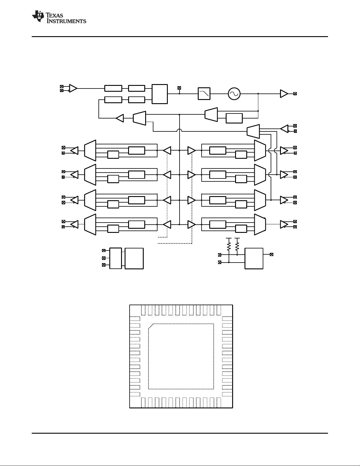
LMK03200 Family Precision 0-Delay Clock Conditioner with Integrated VCO
Check for Samples: LMK03200
1 Introduction
1.1 Features
12
• Integrated VCO with Very Low Phase Noise • Dedicated Divider and Delay Blocks on Each
Floor Clock Output
• Integrated Integer-N PLL with Outstanding • 0-delay Outputs
Normalized Phase Noise Contribution of -224
• Internal or External Feedback of Output Clock
dBc/Hz
• Delay Blocks on N and R Phase Detector Inputs
• VCO Divider Values of 2 to 8 (All Divides)
for Lead/Lag Global Skew Adjust
– Bypassable with VCO Mux When Not in 0-
• Pin Compatible Family of Clocking Devices
delay Mode
• 3.15 to 3.45 V Operation
• Channel Divider Values of 1, 2 to 510 (Even
• Package: 48 Pin WQFN (7.0 x 7.0 x 0.8 mm)
Divides)
• 200 fs RMS Clock Generator Performance (10
• LVDS and LVPECL Clock Outputs
Hz to 20 MHz) with a clean input clock
• Partially Integrated Loop Filter
1.2 Target Applications
• Data Converter Clocking VCO
Device Outputs
Tuning Range RMS Jitter
• Networking, SONET/SDH, DSLAM
(MHz) (fs)
• Wireless Infrastructure
3 LVDS
LMK03200 1185 - 1296 800
• Medical
5 LVPECL
• Test and Measurement
• Military / Aerospace
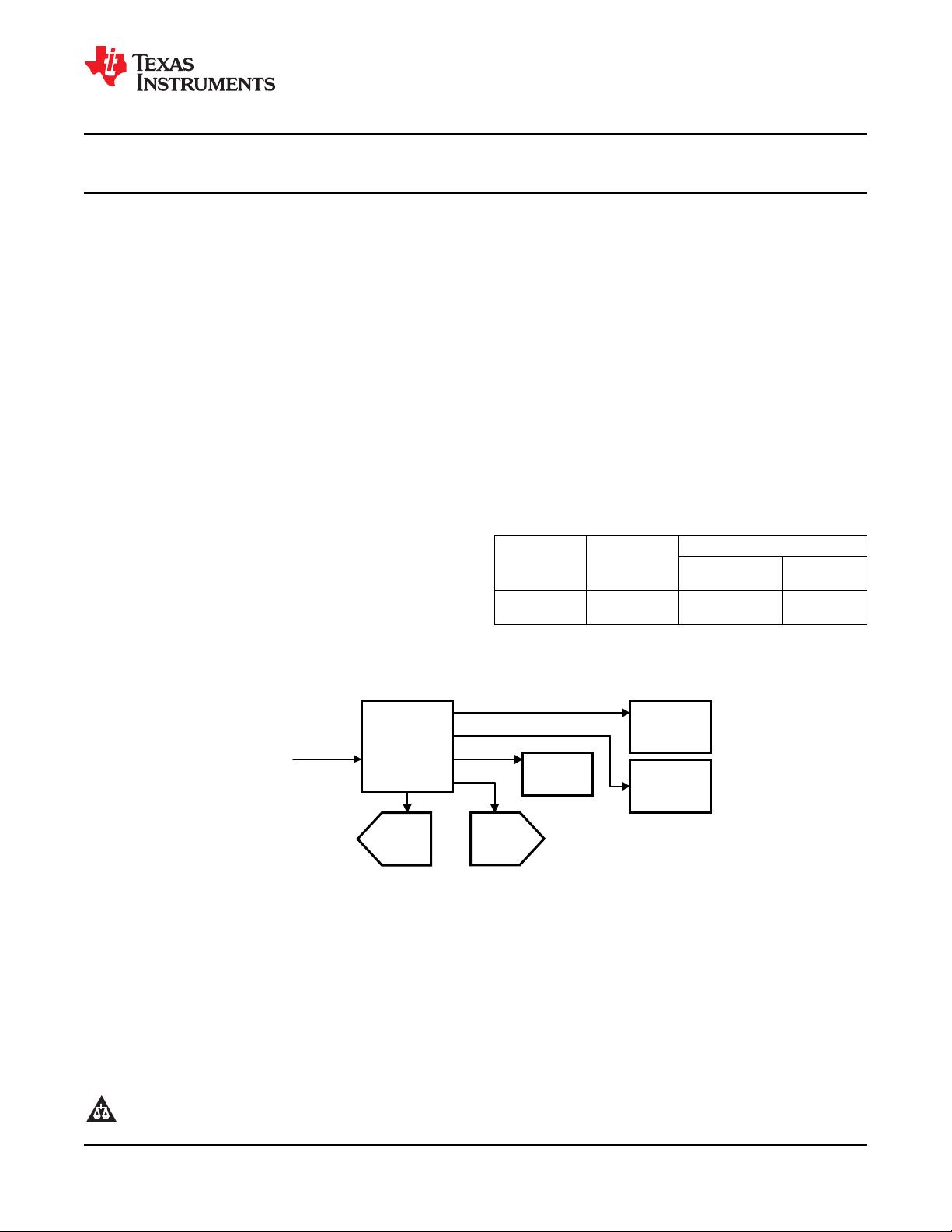
1.3 Description
The LMK03200 family of precision clock conditioners combine the functions of jitter
cleaning/reconditioning, multiplication, and 0-delay distribution of a reference clock. The devices integrate
a Voltage Controlled Oscillator (VCO), a high performance Integer-N Phase Locked Loop (PLL), a partially
integrated loop filter, and up to eight outputs in various LVDS and LVPECL combinations.
The VCO output is optionally accessible on the Fout port. Internally, the VCO output goes through a VCO
divider to feed the various clock distribution blocks.
1
Please be aware that an important notice concerning availability, standard warranty, and use in critical applications of
Texas Instruments semiconductor products and disclaimers thereto appears at the end of this data sheet.
2All trademarks are the property of their respective owners.
PRODUCTION DATA information is current as of publication date. Products conform to
Copyright © 2009–2013, Texas Instruments Incorporated
specifications per the terms of the Texas Instruments standard warranty. Production
processing does not necessarily include testing of all parameters.
LMK03200
SNAS478C –JULY 2009–REVISED APRIL 2013
www.ti.com
Each clock distribution block includes a programmable divider, a phase synchronization circuit, a
programmable delay, a clock output mux, and an LVDS or LVPECL output buffer. The PLL also features
delay blocks to permit global phase adjustment of clock output phase. This allows multiple integer-related
and phase-adjusted copies of the reference to be distributed to eight system components.
The clock conditioners come in a 48-pin WQFN package and are footprint compatible with other clocking
devices in the same family.
1 Introduction .............................................. 1 5.14 0-DELAY MODE .................................... 18
1.1 Features ............................................. 1 6 General Programming Information ................ 19
6.1 Recommended Programming Sequence, without 0-
1.2 Target Applications .................................. 1
Delay Mode ......................................... 19
1.3 Description ........................................... 1
6.2 Recommended Programing Sequence, with 0-Delay
2 Device Information ...................................... 3
Mode ................................................ 19
2.1 Functional Block Diagram ........................... 3
6.3 Recommended Programming Sequence, bypassing
2.2 Connection Diagram ................................. 3
VCO divider ......................................... 23
3 Electrical Specifications ............................... 5
6.4 Register R0 to R7 .................................. 28
3.1 Absolute Maximum Ratings .......................... 5
6.5 Register R8 ......................................... 32
3.2 Recommended Operating Conditions ............... 5
6.6 Register R9 ......................................... 32
3.3 Package Thermal Resistance ....................... 5
6.7 Register R11 ........................................ 32
3.4 Electrical Characteristics ............................ 6
6.8 Register R13 ........................................ 33
3.5 Serial Data Timing Diagram ........................ 10
6.9 Register R14 ........................................ 34
3.6 Charge Pump Current Specification Definitions .... 11
6.10 REGISTER R15 .................................... 37
4 Typical Performance Characteristics ............. 12
7 Application Information .............................. 39
5 Functional Description ............................... 14
7.1 SYSTEM LEVEL DIAGRAM ........................ 39
5.1 BIAS PIN ........................................... 14
7.2 BIAS PIN ........................................... 39
5.2 LDO BYPASS ...................................... 14
7.3 LDO BYPASS ...................................... 39
5.3 OSCILLATOR INPUT PORT (OSCin, OSCin*) .... 14
7.4 LOOP FILTER ...................................... 40
5.4 LOW NOISE, FULLY INTEGRATED VCO ......... 14
7.5 CURRENT CONSUMPTION / POWER
DISSIPATION CALCULATIONS ................... 41
5.5 LVDS/LVPECL OUTPUTS ......................... 15
7.6 THERMAL MANAGEMENT ........................ 42
5.6 GLOBAL CLOCK OUTPUT SYNCHRONIZATION 15
7.7 TERMINATION AND USE OF CLOCK OUTPUTS
5.7 CLKout OUTPUT STATES ......................... 16
(DRIVERS) ......................................... 43
5.8 GLOBAL OUTPUT ENABLE AND LOCK DETECT 16
7.8 OSCin INPUT ...................................... 46
5.9 POWER ON RESET ............................... 16
7.9 MORE THAN EIGHT OUTPUTS WITH AN
5.10 DIGITAL LOCK DETECT ........................... 17
LMK03200 FAMILY DEVICE ....................... 47
5.11 CLKout DELAYS ................................... 17
7.10 DIFFERENTIAL VOLTAGE MEASUREMENT
5.12 GLOBAL DELAYS .................................. 17
TERMINOLOGY .................................... 47
5.13 VCO DIVIDER BYPASS MODE .................... 18
Revision History ............................................ 48
2 Contents Copyright © 2009–2013, Texas Instruments Incorporated
Submit Documentation Feedback
Product Folder Links: LMK03200
4748 46 45 44 43 42 41 40 39 38 37
11
12
10
9
8
7
6
5
4
3
2
1
1413 15 16 17 18 19 20 21 22 23 24
26
25
27
28
29
30
31
32
33
34
35
36GND
Fout
Vcc1
Vcc2
Vcc3
Vcc4
Vcc5
Vcc6
Vcc7
Vcc8
Vcc9
Vcc10
Vcc11
Vcc12
Vcc13
Vcc14
CLKuWire
DATAuWire
LEuWire
NC
LDObyp1
LDObyp2
GOE
LD
CLKout0
CLKout0*
CLKout1
CLKout1*
CLKout2
CLKout2*
CLKout3
CLKout3*
GND
SYNC*
OSCin
OSCin*
CPout
FBCLKin
FBCLKin*
Bias
CLKout4
CLKout4*
CLKout5
CLKout5*
CLKout6
CLKout6*
CLKout7
CLKout7*
DAP
Top Down View
OSCin
OSCin*
R Divider
Phase
Detector
N Divider
CLKout0
CLKout0*
CLKout1
CLKout1*
CLKout2
CLKout2*
CLKout3
CLKout3*
CLKout4
CLKout4*
CLKout5
CLKout5*
CLKout6
CLKout6*
CLKout7
CLKout7*
CPout
Internal
VCO
Partially
Integrated
Loop Filter
Divider
Delay
Mux
Divider
Delay
Mux
Divider
Delay
Mux
Divider
Delay
Mux
Divider
Delay
Mux
Divider
Delay
Mux
Divider
Delay
Mux
Divider
Delay
Mux
Distribution Path
CLK
DATA
LE
Control
Registers
PWire
Port
Device
Control
LDGOE
SYNC*
Fout
Low Clock Buffers
High Clock Buffers
FBCLKin
FBCLKin*
Ndiv
Mux
R Delay
N Delay
FB
Mux
VCO
Mux
VCO
Divider
LMK03200
www.ti.com
SNAS478C –JULY 2009–REVISED APRIL 2013
2 Device Information
2.1 Functional Block Diagram
2.2 Connection Diagram
Figure 2-1. 48-Pin WQFN Package
Copyright © 2009–2013, Texas Instruments Incorporated Device Information 3
Submit Documentation Feedback
Product Folder Links: LMK03200
LMK03200
SNAS478C –JULY 2009–REVISED APRIL 2013
www.ti.com
Table 2-1. PIN DESCRIPTIONS
Pin # Pin Name I/O Description
1, 25 GND - Ground
2 Fout O Internal VCO Frequency Output
3, 8, 13, 16, 19, 22,
Vcc1, Vcc2, Vcc3, Vcc4, Vcc5, Vcc6, Vcc7, Vcc8, Vcc9, Vcc10,
26, 30, 31, 33, 37, - Power Supply
Vcc11, Vcc12, Vcc13, Vcc14
40, 43, 46
4 CLKuWire I MICROWIRE Clock Input
5 DATAuWire I MICROWIRE Data Input
6 LEuWire I MICROWIRE Latch Enable Input
7 NC - No Connection to these pins
9, 10 LDObyp1, LDObyp2 - LDO Bypass
11 GOE I Global Output Enable
12 LD O Lock Detect and Test Output
14, 15 CLKout0, CLKout0* O LVDS Clock Output 0
17, 18 CLKout1, CLKout1* O LVDS Clock Output 1
20, 21 CLKout2, CLKout2* O LVDS Clock Output 2
23, 24 CLKout3, CLKout3* O LVPECL Clock Output 3
27 SYNC* I Global Clock Output Synchronization
Oscillator Clock Input; Should be AC
28, 29 OSCin, OSCin* I
coupled
32 CPout O Charge Pump Output
External Feedback Clock Input for 0-delay
34, 35 FBCLKin, FBCLKin* I
mode
36 Bias I Bias Bypass
38, 39 CLKout4, CLKout4* O LVPECL Clock Output 4
41, 42 CLKout5, CLKout5* O LVPECL Clock Output 5
44, 45 CLKout6, CLKout6* O LVPECL Clock Output 6
47, 48 CLKout7, CLKout7* O LVPECL Clock Output 7
DAP DAP - Die Attach Pad is Ground
4 Device Information Copyright © 2009–2013, Texas Instruments Incorporated
Submit Documentation Feedback
Product Folder Links: LMK03200
LMK03200
www.ti.com
SNAS478C –JULY 2009–REVISED APRIL 2013
These devices have limited built-in ESD protection. The leads should be shorted together or the device placed in conductive foam
during storage or handling to prevent electrostatic damage to the MOS gates.
3 Electrical Specifications
3.1 Absolute Maximum Ratings
(1)(2)(3)
Parameter Symbol Ratings Units
Power Supply Voltage V
CC
-0.3 to 3.6 V
Input Voltage V
IN
-0.3 to (V
CC
+ 0.3) V
Storage Temperature Range T
STG
-65 to 150 °C
Lead Temperature (solder 4 s) T
L
+260 °C
Junction Temperature T
J
125 °C
(1) "Absolute Maximum Ratings" indicate limits beyond which damage to the device may occur, including inoperability and degradation of
device reliability and/or performance. Functional operation of the device and/or non-degradation at the Absolute Maximum Ratings or
other conditions beyond those indicated in the Recommended Operating Conditions is not implied. The Recommended Operating
Conditions indicate conditions at which the device is functional and the device should not be operated beyond such conditions.
(2) This device is a high performance integrated circuit with ESD handling precautions. Handling of this device should only be done at ESD
protected work stations. The device is rated to a HBM-ESD of > 2 kV, a MM-ESD of > 200 V, and a CDM-ESD of > 1.2 kV.
(3) If Military/Aerospace specified devices are required, please contact the Texas Instruments Sales Office/Distributors for availability and
specifications.
3.2 Recommended Operating Conditions
Parameter Symbol Min Typ Max Units
Ambient Temperature T
A
-40 25 85 °C
Power Supply Voltage V
CC
3.15 3.3 3.45 V
3.3 Package Thermal Resistance
Package θ
JA
θ
J-PAD (Thermal Pad)
48-Lead WQFN
(1)
27.4° C/W 5.8° C/W
(1) Specification assumes 16 thermal vias connect the die attach pad to the embedded copper plane on the 4-layer JEDEC board. These
vias play a key role in improving the thermal performance of the WQFN. It is recommended that the maximum number of vias be used in
the board layout.
Copyright © 2009–2013, Texas Instruments Incorporated Electrical Specifications 5
Submit Documentation Feedback
Product Folder Links: LMK03200
剩余55页未读,继续阅读
安全验证
文档复制为VIP权益,开通VIP直接复制
信息提交成功
评论0
最新资源