没有合适的资源?快使用搜索试试~ 我知道了~
TI-LMK04208.pdf
需积分: 5 2 下载量 96 浏览量
2022-11-30
22:47:02
上传
评论 4
收藏 1.59MB PDF 举报
温馨提示
试读
137页
TI-LMK04208.pdf
资源推荐
资源详情
资源评论
Recovered
³GLUW\´FORFNV
or clean clocks
0XOWLSOH³FOHDQ´FORFNVDWGLIIHUHQW
frequencies
CLKout2
CLKout3
CLKout0
FPGA
CLKin0
Crystal or
VCXO
CLKin1
OSCout
CLKout5
DAC
ADC
LMX2582
PLL+VCO
Serializer/
Deserializer
LMK04208
Precision Clock
Conditioner
CLKout1
CPLD
CLKout4
Backup
Reference
Clock
Product
Folder
Sample &
Buy
Technical
Documents
Tools &
Software
Support &
Community
An IMPORTANT NOTICE at the end of this data sheet addresses availability, warranty, changes, use in safety-critical applications,
intellectual property matters and other important disclaimers. PRODUCTION DATA.
English Data Sheet: SNAS684
LMK04208
ZHCSFH1 –SEPTEMBER 2016
LMK04208 具具有有双双环环 PLL 的的低低噪噪声声时时钟钟抖抖动动消消除除器器
1
1 特特性性
1
• 超低的均方根值 (RMS) 抖动性能
– 111fs,RMS 抖动(12kHz 至 20MHz)
– 123fs,RMS 抖动(100Hz 至 20MHz)
• 双环路 PLLatinum™锁相环 (PLL) 架构
• PLL1
– 集成低噪声晶体振荡器电路
– 输入时钟丢失时采用保持模式
– 自动或手动触发/恢复
• PLL2
– 标准化锁相环 (PLL) 噪底为 –227dBc/Hz
– 相位检测器速率最高可达 155MHz
– OSCin 倍频器
– 集成低噪声压控振荡器 (VCO)或外部 VCO 模式
• 两个具有 LOS 的冗余输入时钟
– 自动和手动切换模式
• 50% 占空比输出分配,1 至 1045(偶数和奇数)
• 6 路低电压正射极耦合逻辑 (LVPECL)、低压差分
信令 (LVDS) 或低电压互补金属氧化物半导体
(LVCMOS) 可编程输出
• 数字延迟:固定或可动态调节
• 模拟延迟控制(步长为 25ps)
• 7 路差分输出;最高可达 14 路的单端输出
– 多达 6 个 VCXO/晶振缓冲输出
• 时钟速率高达 1536MHz
• 0 延迟模式
• 加电时 3 个缺省时钟输出
• 多模式:双 PLL、单 PLL 和时钟分配
• 工业温度范围:-40°C 至 +85°C
• 3.15V 至 3.45V 工作电压
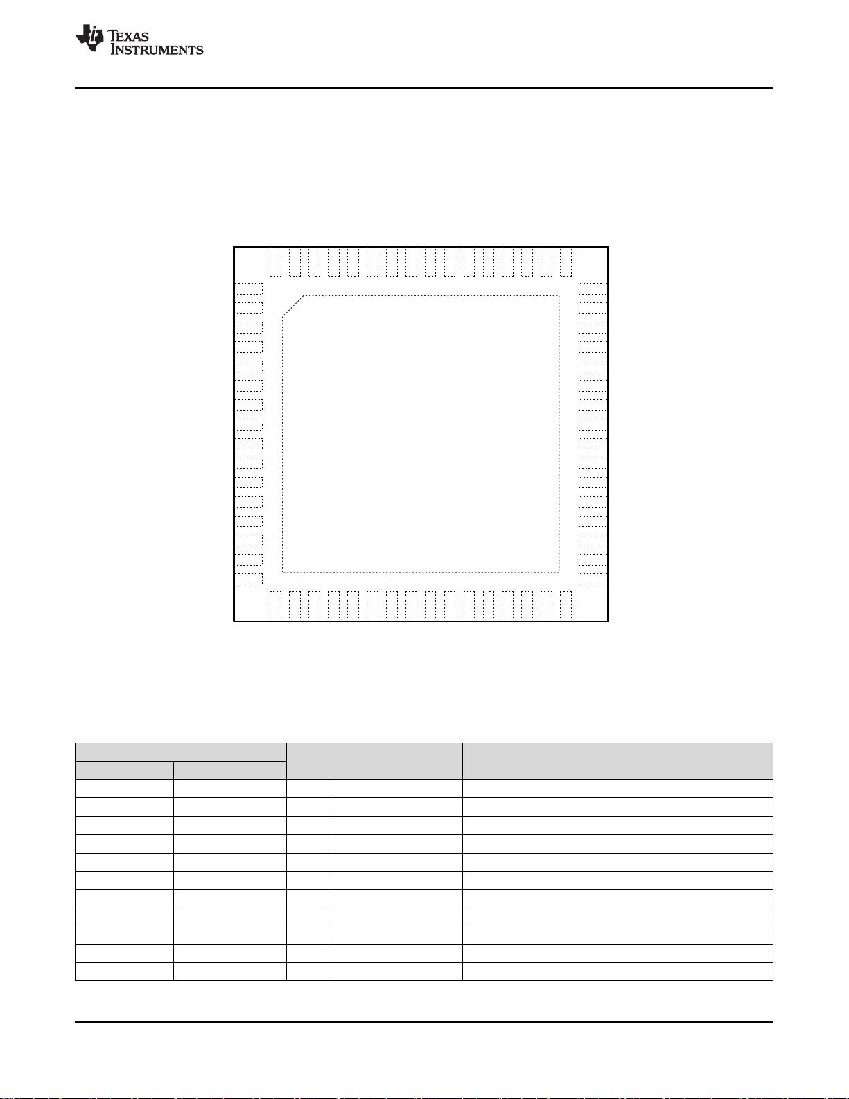
• 64 引脚超薄四方扁平无引线 (WQFN) 封装 (9.0mm
× 9.0mm × 0.8mm)
2 应应用用
• 数据转换器计时
• 无线基础设施
• 网络、同步光纤网 (SONET) 或同步数字体系
(SDH)、数字用户线路接入复用器 (DSLAM)
• 医疗、视频、军事和航天领域
• 测试和测量
3 说说明明
LMK04208 器件是一款高性能时钟调节器,具备出色
的时钟抖动消除、生成和分配 等高级功能, 能够充分
满足新一代系统要求。双环 PLLatinum™架构利用低
噪声 VCXO 模块能够实现 111fs RMS 抖动(12kHz
至 20MHz)或采用低成本外部晶振及变容二极管实现
低于 200fs 的 RMS 抖动(12kHz 至 20MHz)。
双环架构由两个高性能锁相环 (PLL)、一个低噪声晶体
振荡器电路以及一个高性能压控振荡器 (VCO) 构成。
第一个 PLL (PLL1) 具有低噪声抖动消除器功能,而第
二个 PLL (PLL2) 执行时钟生成。PLL1 可配置为与外
部 VCXO 模块配合使用,或与具有外部可调晶体和变
容二极管的集成式晶体振荡器配合使用。当应用于很窄
的环路带宽时,PLL1 使用 VCXO 模块或可调晶体的
优异近端相位噪声(偏移低于 50kHz)清理输入时
钟。PLL1 的输出将用作 PLL2 的清理输入参考,以锁
定集成式 VCO。可对 PLL2 的环路带宽进行优化以清
理远端相位噪声(偏移高于 50 kHz),集成式 VCO
优于 VCXO 模块或 PLL1 中使用的可调晶体。
器器件件信信息息
(1)
器器件件型型号号 VCO 频频率率 时时钟钟输输入入
LMK04208 2750MHz 至 3072MHz 2
(1) 要了解所有可用封装,请见数据表末尾的可订购产品附录。
简简化化电电路路原原理理图图
2
LMK04208
ZHCSFH1 –SEPTEMBER 2016
www.ti.com.cn
Copyright © 2016, Texas Instruments Incorporated
目目录录
1 特特性性.......................................................................... 1
2 应应用用.......................................................................... 1
3 说说明明.......................................................................... 1
4 修修订订历历史史记记录录 ........................................................... 2
5 Pin Configuration and Functions......................... 3
6 Specifications......................................................... 5
6.1 Absolute Maximum Ratings ...................................... 5
6.2 ESD Ratings.............................................................. 5
6.3 Recommended Operating Conditions....................... 5
6.4 Thermal Information.................................................. 6
6.5 Electrical Characteristics........................................... 7
6.6 Timing Requirements.............................................. 13
6.7 Typical Characteristics ........................................... 15
7 Parameter Measurement Information ................ 16
7.1 Charge Pump Current Specification Definitions...... 16
7.2 Differential Voltage Measurement Terminology...... 17
8 Detailed Description............................................ 18
8.1 Overview ................................................................. 18
8.2 Functional Block Diagram ....................................... 22
8.3 Feature Description................................................. 23
8.4 Device Functional Modes........................................ 43
8.5 Programming........................................................... 48
8.6 Register Maps......................................................... 52
9 Application and Implementation ........................ 96
9.1 Application Information............................................ 96
9.2 Typical Applications .............................................. 113
9.3 System Examples ................................................. 121
9.4 Do's and Don'ts..................................................... 123
10 Power Supply Recommendations ................... 124
10.1 Pin Connection Recommendations..................... 124
10.2 Current Consumption and Power Dissipation
Calculations............................................................ 126
11 Layout................................................................. 128
11.1 Layout Guidelines ............................................... 128
11.2 Layout Example .................................................. 129
12 器器件件和和文文档档支支持持 ................................................... 130
12.1 器件支持.............................................................. 130
12.2 文档支持.............................................................. 130
12.3 接收文档更新通知 ............................................... 130
12.4 社区资源.............................................................. 130
12.5 商标 ..................................................................... 130
12.6 静电放电警告....................................................... 130
12.7 Glossary.............................................................. 130
13 机机械械、、封封装装和和可可订订购购信信息息..................................... 130
4 修修订订历历史史记记录录
日日期期 修修订订版版本本 注注释释
2016 年 9 月 * 最初发布。
CLKout4
NC
CLKout5*
Status_CLKin0
CLKout4*
NC
Vcc12
CLKout5
NC
NC
Status_CLKin1
Vcc13
DAP
Top Down View
CLKout3*
Vcc11
NC
NC
NC
Vcc2
Vcc3
NC
Vcc4
NC
CLKout2*
CLKout2
GND
FBCLKin/Fin/CLKin1
FBCLKin*/Fin*/CLKin1*
Status_Holdover
CLKin0
CLKin0*
Vcc5
NC
Vcc7
CPout2
Vcc9
CLKuWire
OSCin*
OSCout
OSCout*
Vcc8
LEuWire
DATAuWire
Vcc10
CLKout3
CPout1
Status_LD
Vcc6
OSCin
NC
NC
NC
CLKout0*
NC
CLKout0
NC
SYNC
NC
NC
Vcc1
LDObyp1
LDObyp2
CLKout1
CLKout1*
NC
48
47
46
45
44
43
42
41
40
39
38
37
36
35
34
33
17
1918 20 21 22 23 24 25 26 27 28 29 30 31
32
1
2
3
4
5
6
7
8
9
10
11
12
13
14
15
16
64
6263 61
60 59
58
57
56 55
54
53 52
51 50 49
3
LMK04208
www.ti.com.cn
ZHCSFH1 –SEPTEMBER 2016
Copyright © 2016, Texas Instruments Incorporated
(1) See Pin Connection Recommendations.
5 Pin Configuration and Functions
NKD Package
64-Pin WQFN with Exposed Pad
Top View
Pin Functions
(1)
PIN
I/O TYPE DESCRIPTION
NO. NAME
1, 2 NC – – No Connection. These pins must be left floating.
3, 4 CLKout0*, CLKout0 O Programmable Clock output 0.
5 NC – – No Connection. These pins must be left floating.
6 SYNC I/O Programmable CLKout Synchronization input or programmable status pin.
7, 8, 9 NC – – No Connection. These pins must be left floating.
10 Vcc1 PWR Power supply for VCO LDO.
11 LDObyp1 ANLG LDO Bypass, bypassed to ground with 10-µF capacitor.
12 LDObyp2 ANLG LDO Bypass, bypassed to ground with a 0.1-µF capacitor.
13, 14 CLKout1, CLKout1* O Programmable Clock output 1.
15, 16 NC – – No Connection. These pins must be left floating.
17 Vcc2 PWR Power supply for clock output 1.
4
LMK04208
ZHCSFH1 –SEPTEMBER 2016
www.ti.com.cn
Copyright © 2016, Texas Instruments Incorporated
Pin Functions
(1)
(continued)
PIN
I/O TYPE DESCRIPTION
NO. NAME
(2) See Vcc5 (CLKin), Vcc7 (OSCin and OSCout) for information on configuring device for optimum performance.
18 Vcc3 PWR Power supply for clock output 2.
19, 20 NC – – No Connection. These pins must be left floating.
21, 22 CLKout2*, CLKout2 O Programmable Clock output 2.
23 GND PWR Ground.
24 Vcc4 PWR Power supply for digital.
25, 26
CLKin1, CLKin1*
I ANLG
Reference Clock Input Port 1 for PLL1. AC or DC Coupled.
FBCLKin, FBCLKin*
Feedback input for external clock feedback input (0-delay
mode). AC or DC Coupled.
Fin/Fin*
External VCO input (External VCO mode). AC or DC
Coupled.
27 Status_Holdover I/O Programmable
Programmable status pin, default readback output.
Programmable to holdover mode indicator. Other options
available by programming.
28, 29 CLKin0, CLKin0* I ANLG
Reference Clock Input Port 0 for PLL1.
AC or DC Coupled.
30 Vcc5 PWR Power supply for clock inputs.
31, 32 NC – – No Connection. These pins must be left floating.
33 Status_LD I/O Programmable
Programmable status pin, default lock detect for PLL1 and
PLL2. Other options available by programming.
34 CPout1 O ANLG Charge pump 1 output.
35 Vcc6 PWR Power supply for PLL1, charge pump 1.
36, 37 OSCin, OSCin* I ANLG
Feedback to PLL1, Reference input to PLL2.
AC Coupled.
38 Vcc7 PWR Power supply for OSCin, OSCout, and PLL2 circuitry.
(2)
39, 40 OSCout, OSCout* O Programmable Buffered output of OSCin port.
(2)
41 Vcc8 PWR Power supply for PLL2, charge pump 2.
42 CPout2 O ANLG Charge pump 2 output.
43 Vcc9 PWR Power supply for PLL2.
44 LEuWire I CMOS MICROWIRE Latch Enable Input.
45 CLKuWire I CMOS MICROWIRE Clock Input.
46 DATAuWire I CMOS MICROWIRE Data Input.
47 Vcc10 PWR Power supply for clock output 3.
48, 49 CLKout3, CLKout3* O Programmable Clock output 3.
50, 51 NC – – No Connection. These pins must be left floating.
52 Vcc11 PWR Power supply for clock output 4.
53, 54 CLKout4, CLKout4* O Programmable Clock output 4.
55, 56 NC – – No Connection. These pins must be left floating.
57 Vcc12 PWR Power supply for clock output 5.
58, 59 CLKout5, CLKout5* O Programmable Clock output 5.
60, 61 NC – – No Connection. These pins must be left floating.
62 Status_CLKin0 I/O Programmable
NC. Programmable status pin. Default is input for pin control
of PLL1 reference clock selection. CLKin0 LOS status and
other options available by programming.
63 Status_CLKin1 I/O Programmable
Programmable status pin. Default is input for pin control of
PLL1 reference clock selection. CLKin1 LOS status and
other options available by programming.
64 Vcc13 PWR Power supply for clock output 0.
DAP DAP – GND DIE ATTACH PAD, connect to GND.
5
LMK04208
www.ti.com.cn
ZHCSFH1 –SEPTEMBER 2016
Copyright © 2016, Texas Instruments Incorporated
(1) Stresses beyond those listed under Absolute Maximum Ratings may cause permanent damage to the device. These are stress ratings
only, which do not imply functional operation of the device at these or any other conditions beyond those indicated under Recommended
Operating Conditions. Exposure to absolute-maximum-rated conditions for extended periods may affect device reliability.
(2) If Military/Aerospace specified devices are required, contact the Texas Instruments Sales Office/Distributors for availability and
specifications.
(3) Never to exceed 3.6 V.
6 Specifications
6.1 Absolute Maximum Ratings
over operating free-air temperature range (unless otherwise noted)
(1)(2)(1)
MIN MAX UNIT
V
CC
Supply voltage
(3)
–0.3 3.6 V
V
IN
Input voltage –0.3 V
CC
+ 0.3 V
T
L
Lead temperature (solder 4 seconds) 260 °C
T
J
Junction temperature 150 °C
I
IN
Differential input current (CLKinX/X*,
OSCin/OSCin*, FBCLKin/FBCLKin*, Fin/Fin*)
± 5 mA
MSL Moisture Sensitivity Level 3
T
stg
Storage temperature -65 150 °C
(1) JEDEC document JEP155 states that 500-V HBM allows safe manufacturing with a standard ESD control process. Manufacturing with
less than 500-V HBM is possible with the necessary precautions. Pins listed as ±2000 V may actually have higher performance.
(2) JEDEC document JEP157 states that 250-V CDM allows safe manufacturing with a standard ESD control process. Manufacturing with
less than 250-V CDM is possible with the necessary precautions. Pins listed as ±750 V may actually have higher performance.
6.2 ESD Ratings
VALUE UNIT
V
(ESD)
Electrostatic discharge
Human-body model (HBM), per ANSI/ESDA/JEDEC JS-001
(1)
±2000
V
Charged-device model (CDM), per JEDEC specification JESD22-
C101
(2)
±750
6.3 Recommended Operating Conditions
MIN NOM MAX UNIT
T
J
Junction temperature 125 °C
T
A
Ambient temperature V
CC
= 3.3 V –40 25 85 °C
V
CC
Supply voltage 3.15 3.3 3.45 V
剩余136页未读,继续阅读
资源评论
不觉明了
- 粉丝: 3156
- 资源: 5416
上传资源 快速赚钱
- 我的内容管理 展开
- 我的资源 快来上传第一个资源
- 我的收益 登录查看自己的收益
- 我的积分 登录查看自己的积分
- 我的C币 登录后查看C币余额
- 我的收藏
- 我的下载
- 下载帮助
安全验证
文档复制为VIP权益,开通VIP直接复制
信息提交成功