TI-LMK02002.pdf
需积分: 9 80 浏览量
2022-11-30
23:33:51
上传
评论 4
收藏 1MB PDF 举报


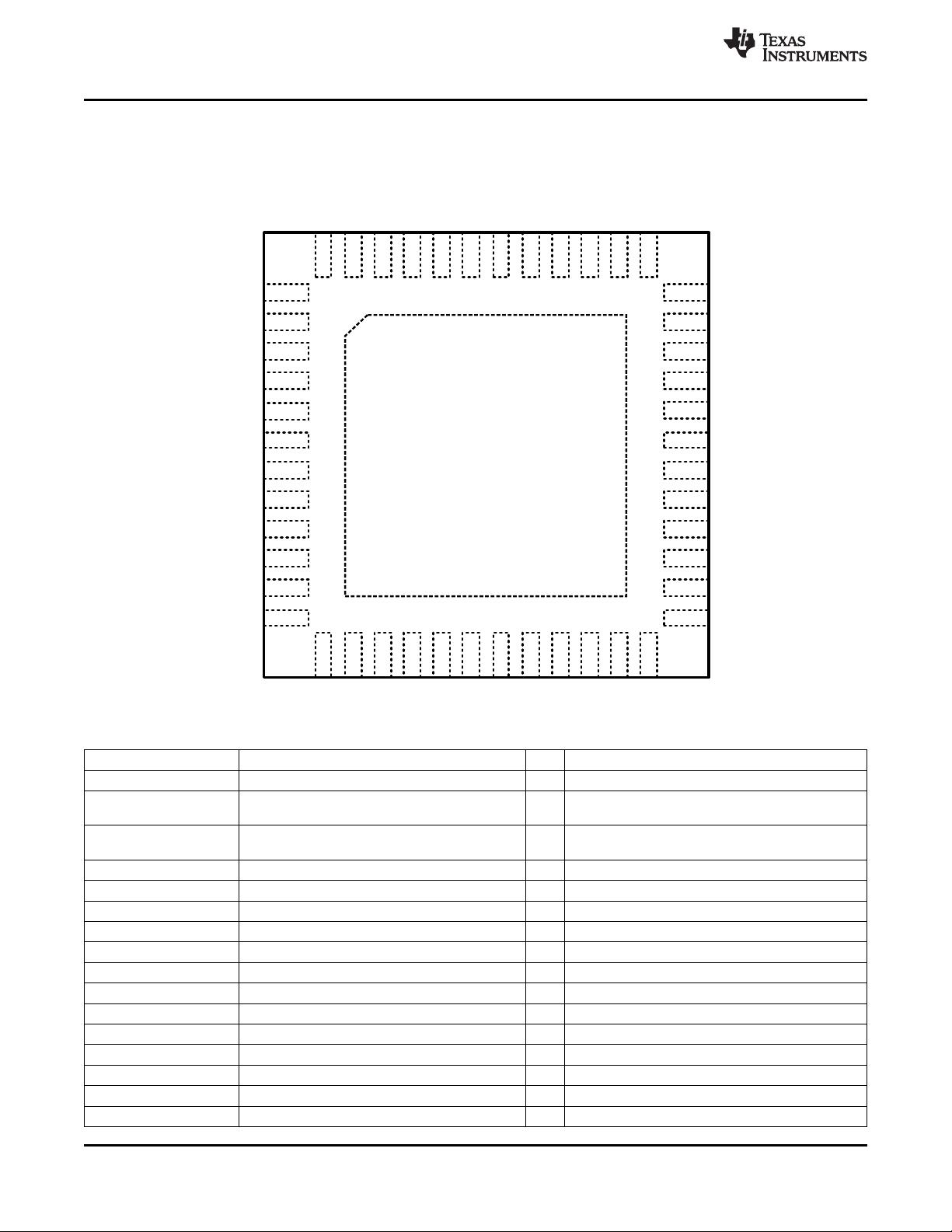
OSCin
OSCin*
R Divider
Phase
Detector
N Divider
CLKout0
CLKout0*
CLKout1
CLKout1*
CLKout2
CLKout2*
CLKout3
CLKout3*
Divider
Delay
Mux
Divider
Delay
Mux
Divider
Delay
Mux
Divider
Delay
Mux
Distribution Path
CLK
DATA
LE
Control
Registers
PWire
Port
Device
Control
LDGOE
SYNC*
CPout
Clock Buffers
Fin
Fin*
Charge
Pump
LMK02002
www.ti.com
SNAS418 –AUGUST 2007
LMK02002 Precision Clock Conditioner with Integrated PLL
Check for Samples: LMK02002
1
FEATURES
DESCRIPTION
The LMK02002 precision clock conditioner combines
2
• 20 fs Additive Jitter
the functions of jitter cleaning/reconditioning,
• Integrated Integer-N PLL with Outstanding
multiplication, and distribution of a reference clock.
Normalized Phase Noise Contribution of -224
The device integrates a high performance Integer-N
dBc/Hz
Phase Locked Loop (PLL), and four LVPECL clock
output distribution blocks.
• Clock Output Frequency Range of 1 to 800
MHz
Each clock distribution block includes a
• 4 LVPECL Clock Outputs
programmable divider, a phase synchronization
circuit, a programmable delay, a clock output mux,
• Dedicated Divider and Delay Blocks on Each
and an LVPECL output buffer. This allows multiple
Clock Output
integer-related and phase-adjusted copies of the
• Pin Compatible Family of Clocking Devices
reference to be distributed to eight system
• 3.15 to 3.45 V Operation
components.
• Package: 48 Pin WQFN (7.0 x 7.0 x 0.8 mm)
The clock conditioner comes in a 48-pin WQFN
package and is footprint compatible with other
TARGET APPLICATIONS
clocking devices in the same family.
• Data Converter Clocking
• Networking, SONET/SDH, DSLAM
• Wireless Infrastructure
• Medical
• Test and Measurement
• Military / Aerospace
Functional Block Diagram
1
Please be aware that an important notice concerning availability, standard warranty, and use in critical applications of
Texas Instruments semiconductor products and disclaimers thereto appears at the end of this data sheet.
2All trademarks are the property of their respective owners.
PRODUCTION DATA information is current as of publication date.
Copyright © 2007, Texas Instruments Incorporated
Products conform to specifications per the terms of the Texas
Instruments standard warranty. Production processing does not
necessarily include testing of all parameters.


剩余24页未读,继续阅读
资源评论


