TI-LMK04133.pdf
需积分: 5 186 浏览量
2022-11-30
22:47:12
上传
评论 4
收藏 1.38MB PDF 举报

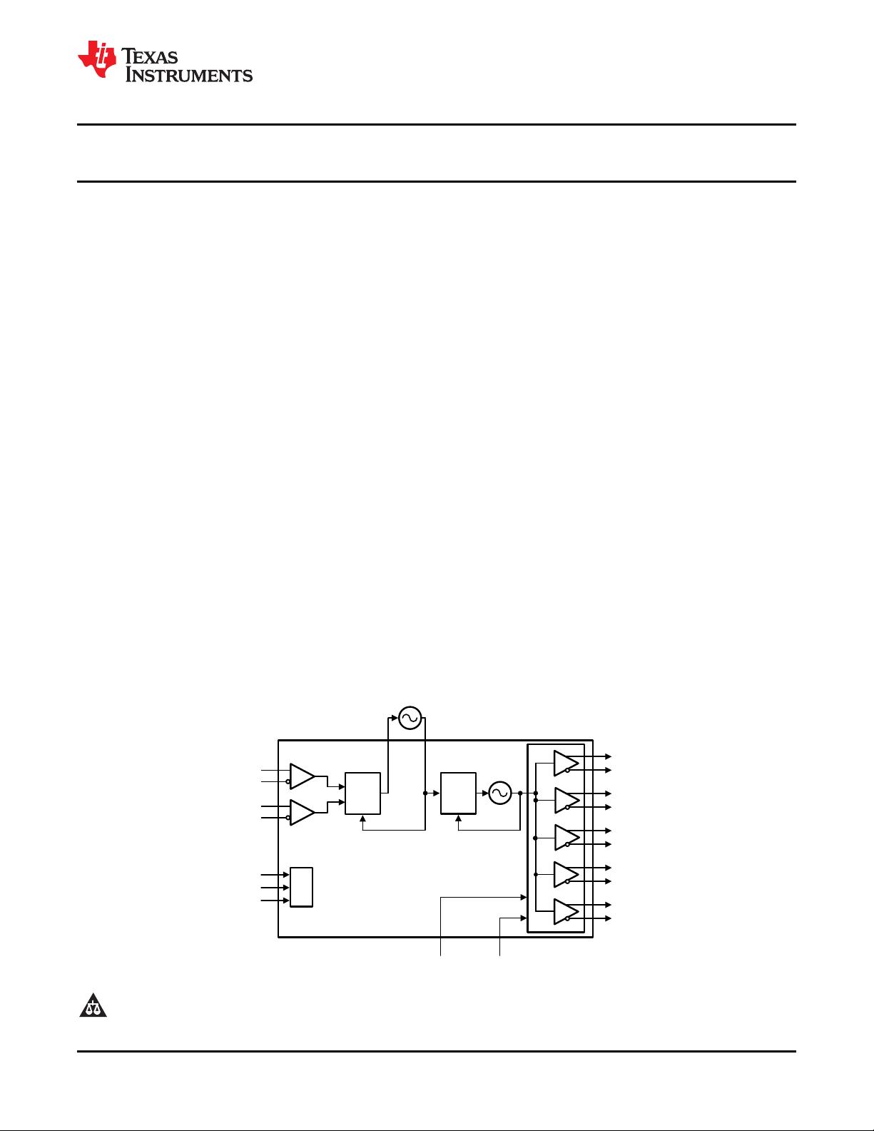
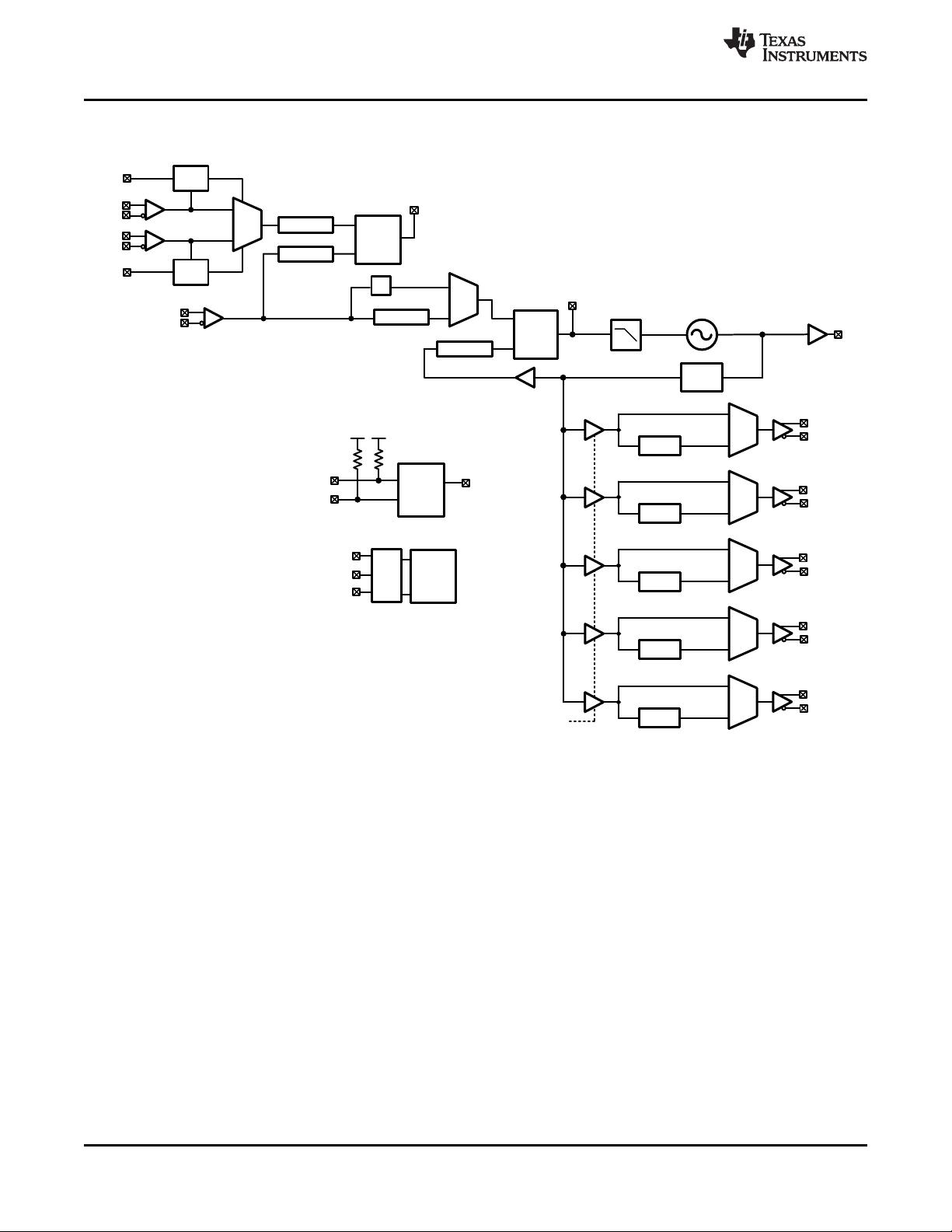
CLK
DATA
LE
PWire
Port
SYNC*
Internal
VCO
CLKin1
PLL1
GOE
PLL2
CLKout0
CLKout1
CLKout2
CLKout3
CLKout4
External VCXO or
low cost crystal
CLKin0
OSCin (Single ended or differential)
LMK04100, LMK04101, LMK04102, LMK04110
LMK04111, LMK04131, LMK04133
www.ti.com
SNAS516B –APRIL 2011–REVISED NOVEMBER 2012
LMK04100 Family Clock Jitter Cleaner with Cascaded PLLs
Check for Samples: LMK04100, LMK04101, LMK04102, LMK04110, LMK04111, LMK04131, LMK04133
1
FEATURES
23
• Cascaded PLLatinum™ PLL Architecture
• Industrial Temperature Range: -40 to 85 °C
– PLL1 • 3.15 V to 3.45 V Operation
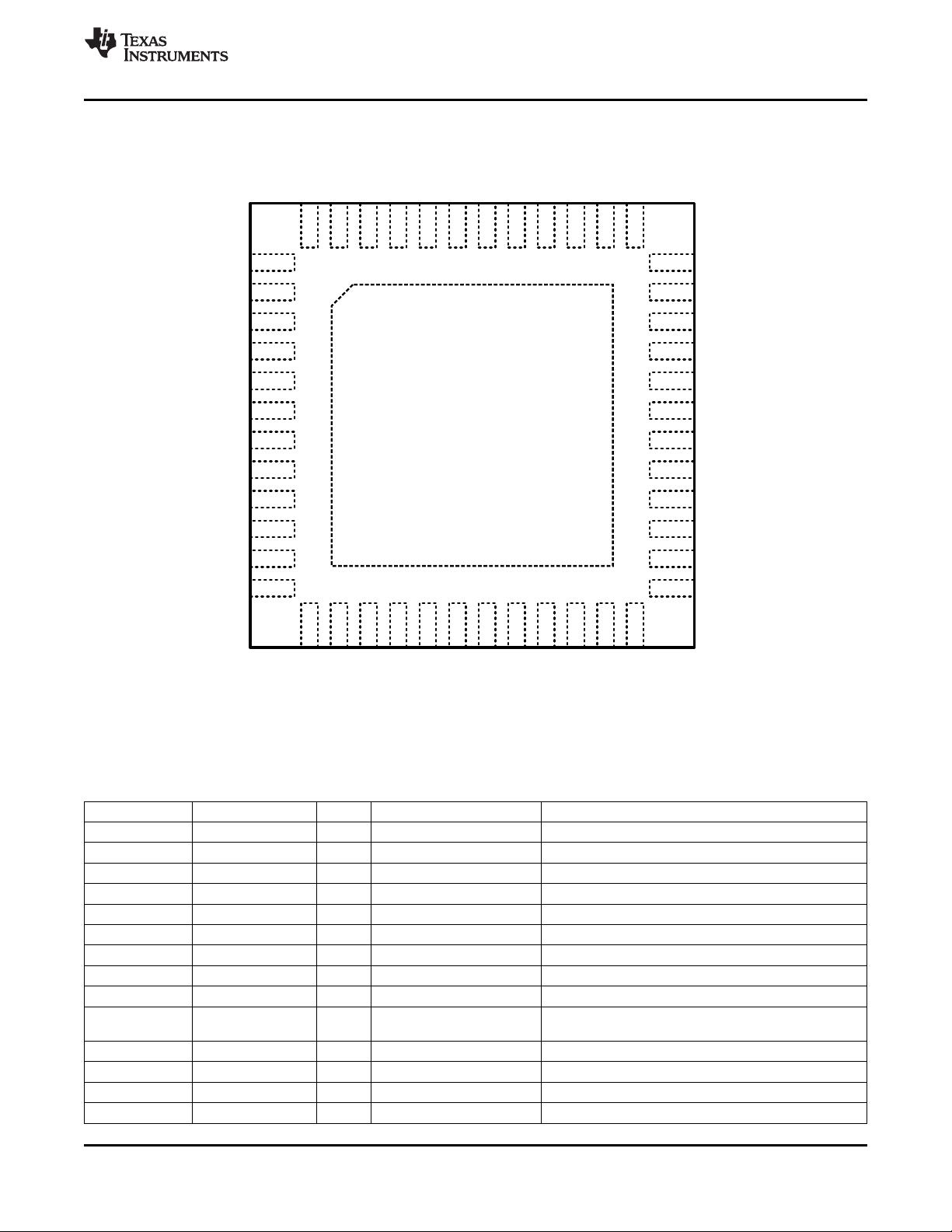
– Redundant Reference Inputs • Package: 48 Pin WQFN (7.0 x 7.0 x 0.8 mm)
– Loss of Signal Detection
APPLICATIONS
– Automatic and Manual Selection of
• Multi-Carrier/Multi-Mode/Multi-Band 2G/3G/4G
Reference Clock Input
Basestations
– PLL2
• Cellular Repeaters
– Phase Detector Rate up to 100 MHz
• High Speed A/D clocking
– Input Frequency-Doubler
• SONET/SDH OC-48/OC-192/OC-768 Line Cards
– Integrated VCO
• GbE/10GbE, 1/2/4/8/10G Fibre Channel Line
• Outputs
Cards
– LVPECL/2VPECL, LVDS, and LVCMOS
• Optical Transport Networks
Formats
• Broadcast Video, HDTV
– Support Clock Rates up to 1080 MHz
• Serial ATA
– Five Dedicated Channel Divider Blocks
– Common Output Frequencies Supported:
DESCRIPTION
– 30.72 MHz, 61.44 MHz, 62.5 MHz, 74.25
The LMK04100 family of precision clock conditioners
MHz, 75 MHz, 77.76 MHz, 100 MHz,
provides jitter cleaning, clock multiplication and
106.25 MHz, 125 MHz, 122.88 MHz, 150
distribution without the need for high-performance
MHz, 155.52 MHz, 156.25 MHz, 159.375
VCXO modules.
MHz, 187.5 MHz, 200 MHz, 212.5 MHz,
When connected to a recovered system reference
245.76 MHz, 250 MHz, 311.04 MHz, 312.5
clock and a VCXO, the device generates 5 low jitter
MHz, 368.64 MHz, 491.52 MHz, 622.08
clocks in LVCMOS, LVDS, or LVPECL formats.
MHz, 625 MHz, 983.04 MHz
• MICROWIRE (SPI) Programming Interface
1
Please be aware that an important notice concerning availability, standard warranty, and use in critical applications of
Texas Instruments semiconductor products and disclaimers thereto appears at the end of this data sheet.
2PLLatinum is a trademark of Texas Instruments.
3All other trademarks are the property of their respective owners.
PRODUCTION DATA information is current as of publication date.
Copyright © 2011–2012, Texas Instruments Incorporated
Products conform to specifications per the terms of the Texas
Instruments standard warranty. Production processing does not
necessarily include testing of all parameters.

剩余53页未读,继续阅读
资源评论


