没有合适的资源?快使用搜索试试~ 我知道了~
TI-SN74S1053.pdf
需积分: 5 0 下载量 54 浏览量
2022-11-29
23:11:09
上传
评论 4
收藏 1.36MB PDF 举报
温馨提示
试读
21页
TI-SN74S1053.pdf
资源推荐
资源详情
资源评论
SN74S1053
16-BIT SCHOTTKY BARRIER DIODE
BUS-TERMINATION ARRAY
SDLS017A – SEPTEMBER 1990 – REVISED AUGUST 1997
1
POST OFFICE BOX 655303 • DALLAS, TEXAS 75265
D
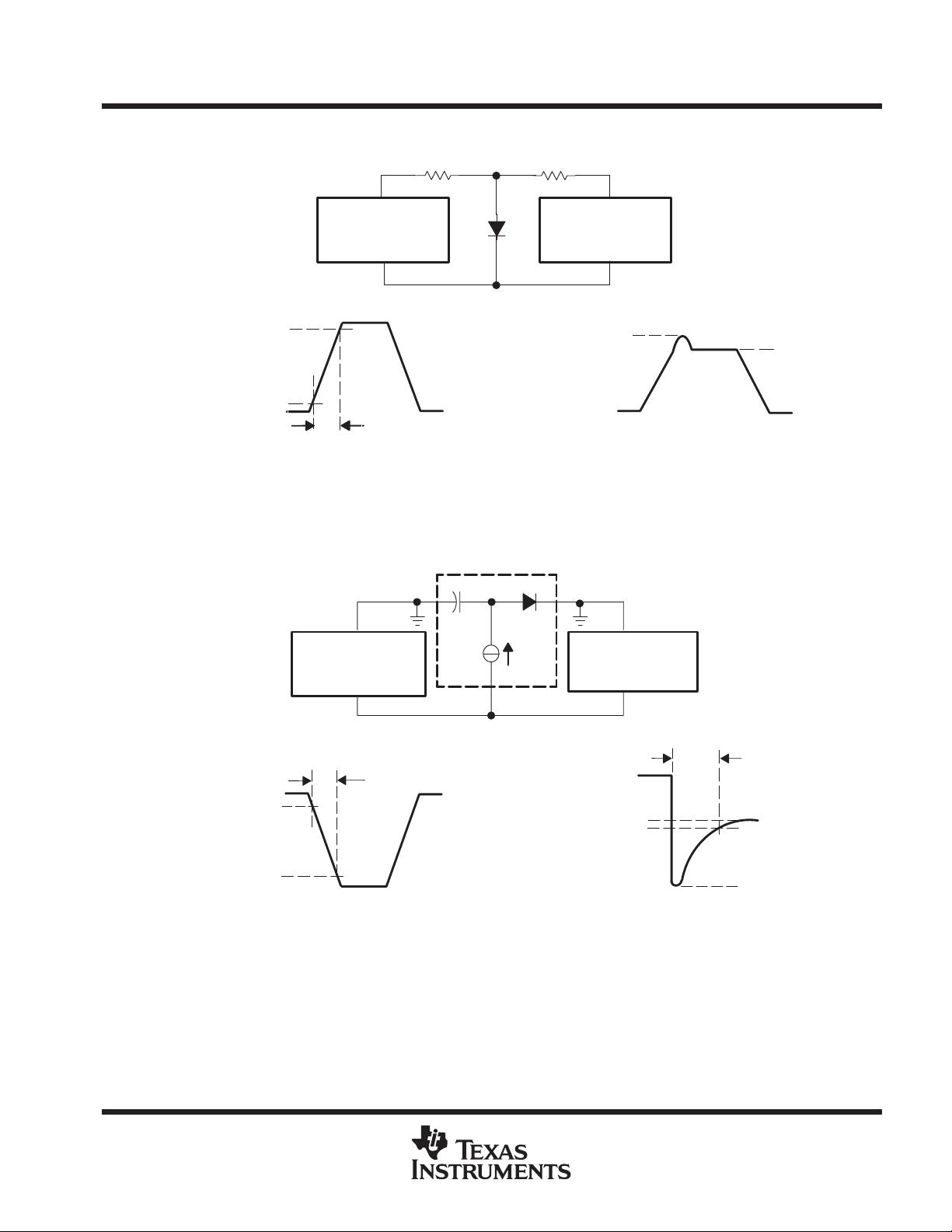
Designed to Reduce Reflection Noise
D
Repetitive Peak Forward Current to 200 mA
D
16-Bit Array Structure Suited for
Bus-Oriented Systems
D
Package Options Include Plastic
Small-Outline Packages and Standard
Plastic 300-mil DIPs
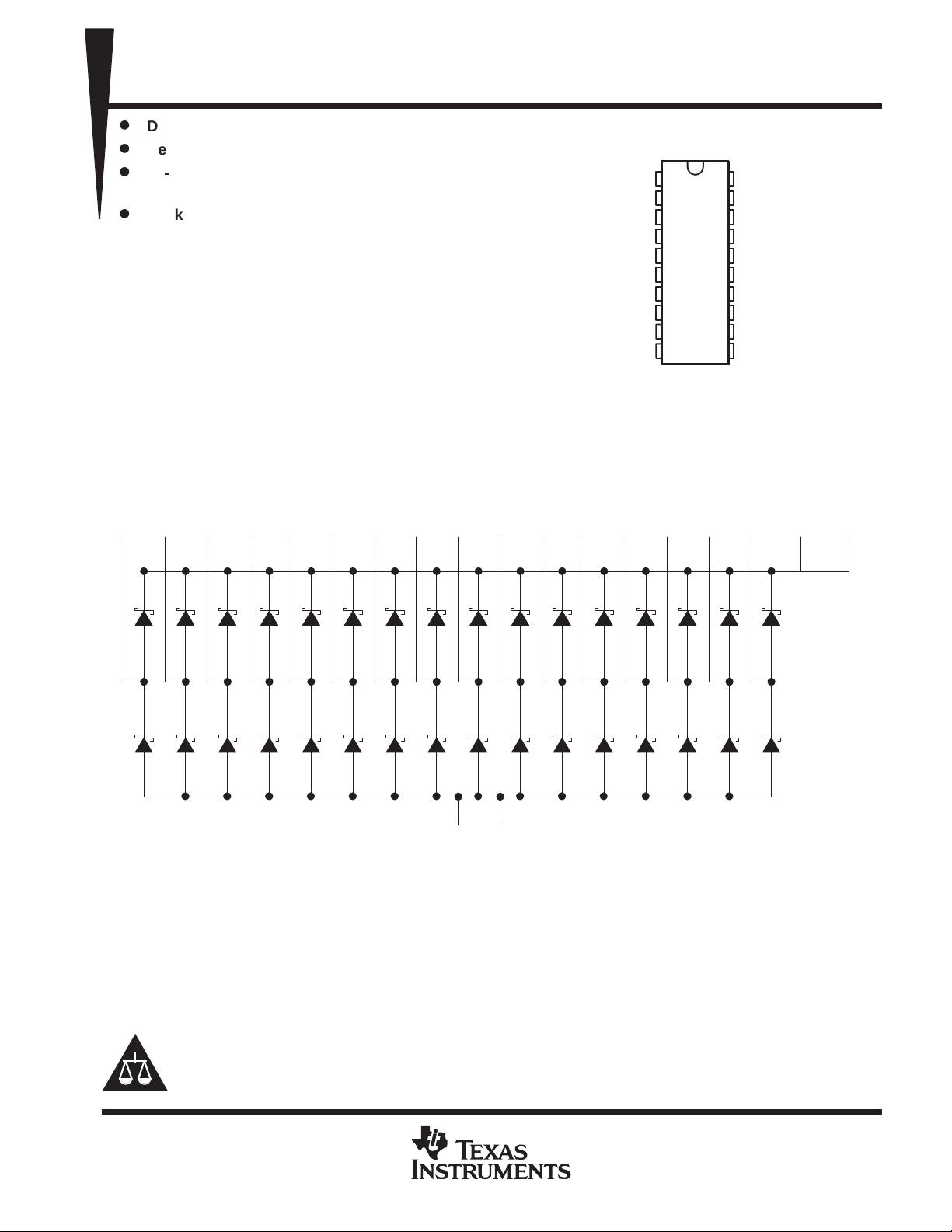
description
This Schottky barrier diode bus-termination array
is designed to reduce reflection noise on memory
bus lines. This device consists of a 16-bit
high-speed Schottky diode array suitable for
clamping to V
CC
and/or GND.
The SN74S1053 is characterized for operation
from 0°C to 70°C.
schematic diagrams
D01
2
D02
3
D03
4
D04
5
D05
6
D06
7
D07
8
D08
9
D09
12
D10
13
D11
14
D12
15
D13
16
D14
17
D15
18
D16
19
10
GND
11
GND
V
CC
1
V
CC
20
Copyright 1997, Texas Instruments Incorporated
PRODUCTION DATA information is current as of publication date.
Products conform to specifications per the terms of Texas Instruments
standard warranty. Production processing does not necessarily include
testing of all parameters.
Please be aware that an important notice concerning availability, standard warranty, and use in critical applications of
Texas Instruments semiconductor products and disclaimers thereto appears at the end of this data sheet.
1
2
3
4
5
6
7
8
9
10
20
19
18
17
16
15
14
13
12
11
V
CC
D01
D02
D03
D04
D05
D06
D07
D08
GND
V
CC
D16
D15
D14
D13
D12
D11
D10
D09
GND
DW OR N PACKAGE
(TOP VIEW)
SN74S1053
16-BIT SCHOTTKY BARRIER DIODE
BUS-TERMINATION ARRAY
SDLS017A – SEPTEMBER 1990 – REVISED AUGUST 1997
2
POST OFFICE BOX 655303 • DALLAS, TEXAS 75265
absolute maximum ratings over operating free-air temperature range (unless otherwise noted)
†
Steady-state reverse voltage, V
R
7 V. . . . . . . . . . . . . . . . . . . . . . . . . . . . . . . . . . . . . . . . . . . . . . . . . . . . . . . . . . . . .
Continuous forward current, I
F
: Any D terminal from GND or to V
CC
50 mA. . . . . . . . . . . . . . . . . . . . . . . . . . .
Total through all GND or V
CC
terminals 170 mA. . . . . . . . . . . . . . . . . . . . . . .
Repetitive peak forward current
‡
, I
FRM
: Any D terminal from GND or V
CC
200 mA. . . . . . . . . . . . . . . . . . . . .
Total through all GND or V
CC
terminals 1.2 A. . . . . . . . . . . . . . . . . .
Continuous total power dissipation at (or below) 25°C free-air temperature (see Note 1) 625 mW. . . . . . . . . .
Operating free-air temperature range 0°C to 70°C. . . . . . . . . . . . . . . . . . . . . . . . . . . . . . . . . . . . . . . . . . . . . . . . . .
Storage temperature range, T
stg
–65°C to 150°C. . . . . . . . . . . . . . . . . . . . . . . . . . . . . . . . . . . . . . . . . . . . . . . . . . .
†
Stresses beyond those listed under “absolute maximum ratings” may cause permanent damage to the device. These are stress ratings only, and
functional operation of the device at these or any other conditions beyond those indicated under “recommended operating conditions” is not
implied. Exposure to absolute-maximum-rated conditions for extended periods may affect device reliability.
‡
These values apply for t
w
≤ 100 µs, duty cycle ≤ 20%.
NOTE 1: For operation above 25°C free-air temperature, derate linearly at the rate of 5 m/W/°C.
electrical characteristics over recommended operating free-air temperature range (unless
otherwise noted)
single-diode operation (see Note 2)
PARAMETER TEST CONDITIONS MIN TYP
§
MAX UNIT
To V
CC
I
F
= 18 mA 0.85 1.05
V
F
Static forward voltage
To
V
CC
I
F
= 50 mA 1.05 1.3
V
V
F
Static
for
w
ard
v
oltage
From GND
I
F
= 18 mA 0.75 0.95
V
From
GND
I
F
= 50 mA 0.95 1.2
V
FM
Peak forward voltage I
F
= 200 mA 1.45 V
I
R
Static reverse current
To V
CC
V
R
=7V
5
µA
I
R
Static
re
v
erse
c
u
rrent
From GND
V
R
=
7
V
5
µ
A
C
t
Total ca
p
acitance
V
R
= 0 V, f = 1 MHz 8 16
p
F
C
t
Total
capacitance
V
R
= 2 V, f = 1 MHz 4 8
pF
§
All typical values are at V
CC
= 5 V, T
A
= 25°C.
NOTE 2: Test conditions and limits apply separately to each of the diodes. The diodes not under test are open-circuited during the measurement
of these characteristics.
multiple-diode operation
PARAMETER TEST CONDITIONS MIN TYP
‡
MAX UNIT
I
Internal crosstalk current
Total I
F
current = 1 A, See Note 3 0.8 2
mA
I
x
Internal
crosstalk
c
u
rrent
Total I
F
current = 198 mA, See Note 3 0.02 0.2
mA
§
All typical values are at V
CC
= 5 V, T
A
= 25°C.
NOTE 3: I
x
is measured under the following conditions with one diode static, and all others switching:
Switching diodes: t
w
= 100 µs, duty cycle = 20%
Static diode: V
R
= 5 V
The static diode input current is the internal crosstalk current I
x
.
switching characteristics, T
A
= 25°C (see Figures 1 and 2)
PARAMETER TEST CONDITIONS MIN TYP MAX UNIT
t
rr
Reverse recovery time I
F
= 10 mA, I
RM(REC)
= 10 mA, I
R(REC)
= 1 mA, R
L
= 100 Ω 8 16 ns
SN74S1053
16-BIT SCHOTTKY BARRIER DIODE
BUS-TERMINATION ARRAY
SDLS017A – SEPTEMBER 1990 – REVISED AUGUST 1997
3
POST OFFICE BOX 655303 • DALLAS, TEXAS 75265
PARAMETER MEASUREMENT INFORMATION
90%
10%
DUT
t
r
V
FM
(See Note A) (See Note B)
50 Ω
450 Ω
Pulse
Generator
V
F
Sampling
Oscilloscope
Input Pulse
(See Note A)
Output
Waveform
(See Note B)
NOTES: A. The input pulse is supplied by a pulse generator having the following characteristics: t
r
= 20 ns, Z
O
= 50 Ω, freq = 500 Hz,
duty cycle = 1%.
B. The output waveform is monitored by an oscilloscope having the following characteristics: t
r
≤ 350 ps, R
i
= 50 Ω, C
i
≤ 5 pF.
Figure 1. Forward Recovery Voltage
I
F
DUT
90%
10%
t
f
I
f
Pulse
Generator
(See Note A)
(See Note B)
I
R(REC)
t
rr
I
RM(REC)
Sampling
Oscilloscope
Input Pulse
(See Note A)
Output
Waveform
(See Note B)
0
NOTES: A. The input pulse is supplied by a pulse generator having the following characteristics: t
f
= 0.5 ns, Z
O
= 50 Ω, t
w
≥ 50 ns,
duty cycle = 1%.
B. The output waveform is monitored by an oscilloscope having the following characteristics: t
r
≤ 350 ps, R
i
= 50 Ω, C
i
≤ 5 pF.
Figure 2. Reverse Recovery Time
SN74S1053
16-BIT SCHOTTKY BARRIER DIODE
BUS-TERMINATION ARRAY
SDLS017A – SEPTEMBER 1990 – REVISED AUGUST 1997
4
POST OFFICE BOX 655303 • DALLAS, TEXAS 75265
APPLICATION INFORMATION
Large negative transients occurring at the inputs of memory devices (DRAMs, SRAMs, EPROMs, etc.) or on the
CLOCK lines of many clocked devices can result in improper operation of the devices. The SN74S1053 diode
termination array helps suppress negative transients caused by transmission-line reflections, crosstalk, and
switching noise.
Diode terminations have several advantages when compared to resistor termination schemes. Split resistor or
Thevenin equivalent termination can cause a substantial increase in power consumption. The use of a single resistor
to ground to terminate a line usually results in degradation of the output high level, resulting in reduced noise immunity.
Series damping resistors placed on the outputs of the driver reduce negative transients, but they also can increase
propagation delays down the line, as a series resistor reduces the output drive capability of the driving device. Diode
terminations have none of these drawbacks.
The operation of the diode arrays in reducing negative transients is explained in the following figures. The diode
conducts current when the voltage reaches a negative value large enough for the diode to turn on. Suppression of
negative transients is tracked by the current-voltage characteristic curve for that diode. Typical current versus voltage
curves for the SN74S1053 are shown in Figures 3 and 4.
To illustrate how the diode arrays act to reduce negative transients at the end of a transmission line, the test setup
in Figure 5 was evaluated. The resulting waveforms with and without the diode are shown in Figure 6.
The maximum effectiveness of the diode arrays in suppressing negative transients occurs when the diode arrays are
placed at the end of a line and/or the end of a long stub branching off a main transmission line. The diodes also can
be used to reduce the negative transients that occur due to discontinuities in the middle of a line. An example of this
is a slot in a backplane that is provided for an add-on card.
– Forward Current – mA
V
I
– Forward Voltage – V
I
I
DIODE FORWARD CURRENT
vs
DIODE FORWARD VOLTAGE
–50
–40
–20
–10
0
–90
–30
0 0.2 0.4 0.6 0.8 1 1.2
–70
–60
–80
–100
1.4 1.6 1.8 2
T
A
= 25°C
Figure 3. Typical Input Current vs Input Voltage
(Lower Diode)
SN74S1053
16-BIT SCHOTTKY BARRIER DIODE
BUS-TERMINATION ARRAY
SDLS017A – SEPTEMBER 1990 – REVISED AUGUST 1997
5
POST OFFICE BOX 655303 • DALLAS, TEXAS 75265
– Forward Current – mA
V
I
– Forward Voltage – V
I
I
DIODE FORWARD CURRENT
vs
DIODE FORWARD VOLTAGE
50
40
20
10
0
90
30
0 0.2 0.4 0.6 0.8 1 1.2
70
60
80
100
1.4 1.6 1.8 2
T
A
= 25°C
Figure 4. Typical Input Current vs Input Voltage
(Upper Diode)
剩余20页未读,继续阅读
资源评论
不觉明了
- 粉丝: 3164
- 资源: 5429
上传资源 快速赚钱
- 我的内容管理 展开
- 我的资源 快来上传第一个资源
- 我的收益 登录查看自己的收益
- 我的积分 登录查看自己的积分
- 我的C币 登录后查看C币余额
- 我的收藏
- 我的下载
- 下载帮助
安全验证
文档复制为VIP权益,开通VIP直接复制
信息提交成功