没有合适的资源?快使用搜索试试~ 我知道了~
TI-SN74S00.pdf
需积分: 10 0 下载量 125 浏览量
2022-11-27
17:06:54
上传
评论 4
收藏 1.47MB PDF 举报
温馨提示
试读
34页
TI-SN74S00.pdf
资源详情
资源评论
A
B
Y
Product
Folder
Order
Now
Technical
Documents
Tools &
Software
Support &
Community
An IMPORTANT NOTICE at the end of this data sheet addresses availability, warranty, changes, use in safety-critical applications,
intellectual property matters and other important disclaimers. PRODUCTION DATA.
SN5400
,
SN54LS00
,
SN54S00
SN7400
,
SN74LS00
,
SN74S00
SDLS025D –DECEMBER 1983–REVISED MAY 2017
SNx400, SNx4LS00, and SNx4S00 Quadruple 2-Input Positive-NAND Gates
1
1 Features
1
• Package Options Include:
– Plastic Small-Outline (D, NS, PS)
– Shrink Small-Outline (DB)
– Ceramic Flat (W)
– Ceramic Chip Carriers (FK)
– Standard Plastic (N)
– Ceramic (J)
• Also Available as Dual 2-Input Positive-NAND
Gate in Small-Outline (PS) Package
• Inputs Are TTL Compliant; V
IH
= 2 V and
V
IL
= 0.8 V
• Inputs Can Accept 3.3-V or 2.5-V Logic Inputs
• SN5400, SN54LS00, and SN54S00 are
Characterized For Operation Over the Full Military
Temperature Range of –55ºC to 125ºC
2 Applications
• AV Receivers
• Portable Audio Docks
• Blu-Ray Players
• Home Theater
• MP3 Players or Recorders
• Personal Digital Assistants (PDAs)
3 Description
The SNx4xx00 devices contain four independent,
2-input NAND gates. The devices perform the
Boolean function Y = A .B or Y = A + B in positive
logic.
Device Information
(1)
PART NUMBER PACKAGE BODY SIZE (NOM)
SN74LS00DB SSOP (14) 6.20 mm × 5.30 mm
SN7400D,
SN74LS00D,
SN74S00D
SOIC (14) 8.65 mm × 3.91 mm
SN74LS00NSR PDIP (14) 19.30 × 6.35 mm
SNJ5400J,
SNJ54LS00J,
SNJ54S00J
CDIP (14) 19.56 mm × 6.67 mm
SNJ5400W,
SNJ54LS00W,
SNJ54S00W
CFP (14) 9.21 mm × 5.97 mm
SN54LS00FK,
SN54S00FK
LCCC (20) 8.89 mm × 8.89 mm
SN7400NS,
SN74LS00NS,
SN74S00NS
SO (14) 10.30 mm × 5.30 mm
SN7400PS,
SN74LS00PS
SO (8) 6.20 mm × 5.30 mm
(1) For all available packages, see the orderable addendum at
the end of the data sheet.
Logic Diagram, Each Gate (Positive Logic)
2
SN5400
,
SN54LS00
,
SN54S00
SN7400
,
SN74LS00
,
SN74S00
SDLS025D –DECEMBER 1983–REVISED MAY 2017
www.ti.com
Product Folder Links: SN5400 SN54LS00 SN54S00 SN7400 SN74LS00 SN74S00
Submit Documentation Feedback Copyright © 1983–2017, Texas Instruments Incorporated
Table of Contents
1 Features.................................................................. 1
2 Applications ........................................................... 1
3 Description ............................................................. 1
4 Revision History..................................................... 2
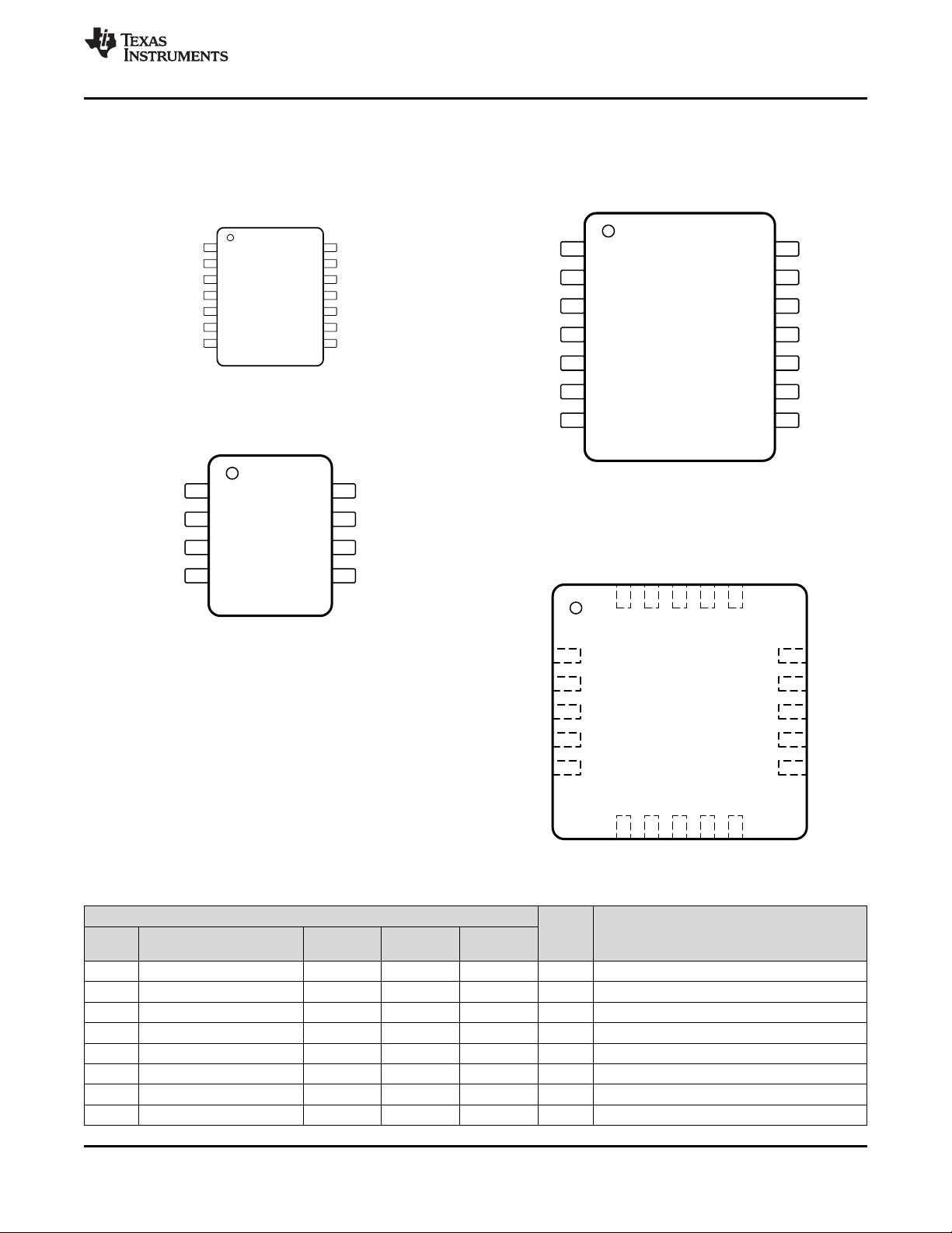
5 Pin Configuration and Functions......................... 3
6 Specifications......................................................... 4
6.1 Absolute Maximum Ratings ...................................... 4
6.2 ESD Ratings: SN74LS00.......................................... 4
6.3 Recommended Operating Conditions....................... 4
6.4 Thermal Information.................................................. 6
6.5 Electrical Characteristics: SNx400............................ 6
6.6 Electrical Characteristics: SNx4LS00 ....................... 6
6.7 Electrical Characteristics: SNx4S00 ......................... 6
6.8 Switching Characteristics: SNx400 ........................... 7
6.9 Switching Characteristics: SNx4LS00....................... 7
6.10 Switching Characteristics: SNx4S00....................... 7
6.11 Typical Characteristics............................................ 8
7 Parameter Measurement Information .................. 9
7.1 Propagation Delays, Setup and Hold Times, and
Pulse Width................................................................ 9
8 Detailed Description............................................ 10
8.1 Overview ................................................................. 10
8.2 Functional Block Diagram ....................................... 10
8.3 Feature Description................................................. 10
8.4 Device Functional Modes....................................... 10
9 Application and Implementation ........................ 11
9.1 Application Information............................................ 11
9.2 Typical Application .................................................. 11
10 Power Supply Recommendations ..................... 12
11 Layout................................................................... 13
11.1 Layout Guidelines ................................................. 13
11.2 Layout Example .................................................... 13
12 Device and Documentation Support ................. 14
12.1 Documentation Support ........................................ 14
12.2 Related Links ........................................................ 14
12.3 Receiving Notification of Documentation Updates 14
12.4 Community Resources.......................................... 14
12.5 Trademarks........................................................... 14
12.6 Electrostatic Discharge Caution............................ 14
12.7 Glossary................................................................ 14
13 Mechanical, Packaging, and Orderable
Information ........................................................... 15
4 Revision History
NOTE: Page numbers for previous revisions may differ from page numbers in the current version.
Changes from Revision C (November 2016) to Revision D Page
• Changed Typical Application Diagram see Application and Implementation section............................................................. 1
Changes from Revision B (October 2003) to Revision C Page
• Added ESD Ratings table, Feature Description section, Device Functional Modes, Application and Implementation
Power Supply Recommendations section, Layout section, Device and Documentation Support section, and
Mechanical, Packaging, and Orderable Information section.................................................................................................. 1
• Changed Ordering Information table to Device Comparison Table; see Package Option Addendum at the end of the
data sheet............................................................................................................................................................................... 1
• Changed Package thermal impedance, R
θJA
, values in Thermal Information table From: 86°C/W To: 90.9°C/W (D),
From: 96°C/W To: 102.8°C/W (DB), From: 80°C/W To: 54.8°C/W (N), and From: 76°C/W To: 89.7°C/W (NS)................... 6
41Y
5NC
62A
7NC
82B
92Y
10
GND
11
NC
12
3Y
13
3A
14 3B
15 NC
16 4Y
17 NC
18 4A
19 4B
20 V
CC
1 NC
2 1A
3 1B
Not to scale
11A 8 V
CC
21B 7 2B
31Y 6 2A
4GND 5 2Y
Not to scale
11A 14 4Y
21B 13 4B
31Y 12 4A
4V
CC
11 GND
52Y 10 3B
62A 9 3A
72B 8 3Y
Not to scale
11A 14 V
CC
21B 13 4A
31Y 12 4B
42A 11 4Y
52B 10 3A
62Y 9 3B
7GND 8 3Y
Not to scale
3
SN5400
,
SN54LS00
,
SN54S00
SN7400
,
SN74LS00
,
SN74S00
www.ti.com
SDLS025D –DECEMBER 1983–REVISED MAY 2017
Product Folder Links: SN5400 SN54LS00 SN54S00 SN7400 SN74LS00 SN74S00
Submit Documentation FeedbackCopyright © 1983–2017, Texas Instruments Incorporated
5 Pin Configuration and Functions
SN5400 J, SN54xx00 J and W, SN74x00 D, N, and NS, or
SN74LS00 D, DB, N, and NS Packages
14-Pin CDIP, CFP, SOIC, PDIP, SO, or SSOP
Top View
SN5400 W Package
14-Pin CFP
Top View
SN74xx00 PS Package
18-Pin SO
Top View
SN54xx00 FK Package
20-Pin LCCC
Top View
Pin Functions
PIN
I/O DESCRIPTION
NAME
CDIP, CFP, SOIC,
PDIP, SO, SSOP
SO
(SN74xx00)
CFP
(SN5400)
LCCC
1A 1 1 1 2 I Gate 1 input
1B 2 2 2 3 I Gate 1 input
1Y 3 3 3 4 O Gate 1 output
2A 4 6 6 6 I Gate 2 input
2B 5 7 7 8 I Gate 2 input
2Y 6 5 5 9 O Gate 2 output
3A 10 — 9 13 I Gate 3 input
3B 9 — 10 14 I Gate 3 input
4
SN5400
,
SN54LS00
,
SN54S00
SN7400
,
SN74LS00
,
SN74S00
SDLS025D –DECEMBER 1983–REVISED MAY 2017
www.ti.com
Product Folder Links: SN5400 SN54LS00 SN54S00 SN7400 SN74LS00 SN74S00
Submit Documentation Feedback Copyright © 1983–2017, Texas Instruments Incorporated
Pin Functions (continued)
PIN
I/O DESCRIPTION
NAME
CDIP, CFP, SOIC,
PDIP, SO, SSOP
SO
(SN74xx00)
CFP
(SN5400)
LCCC
3Y 8 — 8 12 O Gate 3 output
4A 13 — 12 18 I Gate 4 input
4B 12 — 13 19 I Gate 4 input
4Y 11 — 14 16 O Gate 4 output
GND 7 4 11 10 — Ground
NC — — —
1, 5, 7,
11, 15, 17
— No connect
V
CC
14 8 4 20 — Power supply
(1) Stresses beyond those listed under Absolute Maximum Ratings may cause permanent damage to the device. These are stress ratings
only, which do not imply functional operation of the device at these or any other conditions beyond those indicated under Recommended
Operating Conditions. Exposure to absolute-maximum-rated conditions for extended periods may affect device reliability.
(2) Voltage values are with respect to network ground terminal.
6 Specifications
6.1 Absolute Maximum Ratings
over operating free-air temperature range (unless otherwise noted)
(1)
MIN MAX UNIT
Supply voltage, V
CC
(2)
7 V
Input voltage
SNx400 and SNxS400 5.5
V
SNx4LS00 7
Junction temperature, T
J
150 °C
Storage temperature, T
stg
–65 150 °C
(1) JEDEC document JEP155 states that 500-V HBM allows safe manufacturing with a standard ESD control process. Manufacturing with
less than 500-V HBM is possible with the necessary precautions.
(2) JEDEC document JEP157 states that 250-V CDM allows safe manufacturing with a standard ESD control process. Manufacturing with
less than 250-V CDM is possible with the necessary precautions. Pins listed as ±2000 V may actually have higher performance. ESD
Tested on SN74LS00N package.
6.2 ESD Ratings: SN74LS00
VALUE UNIT
V
(ESD)
Electrostatic
discharge
Human-body model (HBM), per ANSI/ESDA/JEDEC JS-001
(1)
±500
V
Charged-device model (CDM), per JEDEC specification JESD22-C101
(2)
±2000
6.3 Recommended Operating Conditions
over operating free-air temperature range (unless otherwise noted)
MIN NOM MAX UNIT
V
CC
Supply voltage
SN54xx00 4.5 5 5.5
V
SN74xx00 4.75 5 5.25
V
IH
High-level input voltage 2 V
V
IL
Low-level input voltage
SNx400, SN7LS400, and SNx4S00 0.8
V
SN54LS00 0.7
I
OH
High-level output current
SN5400, SN54LS00, and SN74LS00 –0.4
mA
SNx4S00 –1
I
OL
Low-level output current
SNx400 16
mA
SN5LS400 4
SN7LS400 8
SNx4S00 20
5
SN5400
,
SN54LS00
,
SN54S00
SN7400
,
SN74LS00
,
SN74S00
www.ti.com
SDLS025D –DECEMBER 1983–REVISED MAY 2017
Product Folder Links: SN5400 SN54LS00 SN54S00 SN7400 SN74LS00 SN74S00
Submit Documentation FeedbackCopyright © 1983–2017, Texas Instruments Incorporated
Recommended Operating Conditions (continued)
over operating free-air temperature range (unless otherwise noted)
MIN NOM MAX UNIT
T
A
Operating free-air temperature
SN54xx00 –55 125
°C
SN74xx00 0 70
剩余33页未读,继续阅读
安全验证
文档复制为VIP权益,开通VIP直接复制
信息提交成功
评论0
最新资源