TI-SN74ACT7882.pdf
需积分: 10 78 浏览量
2022-12-11
13:58:07
上传
评论 5
收藏 198KB PDF 举报
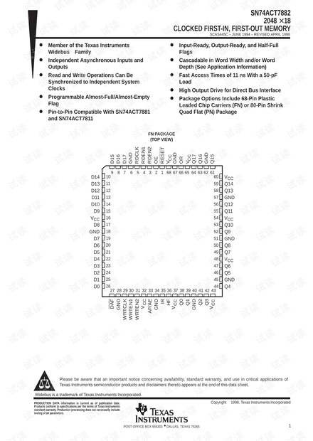
SN74ACT7882
2048 × 18
CLOCKED FIRST-IN, FIRST-OUT MEMORY
SCAS445C – JUNE 1994 – REVISED APRIL 1998
1
POST OFFICE BOX 655303 • DALLAS, TEXAS 75265
D
Member of the Texas Instruments
Widebus Family
D
Independent Asynchronous Inputs and
Outputs
D
Read and Write Operations Can Be
Synchronized to Independent System
Clocks
D
Programmable Almost-Full/Almost-Empty
Flag
D
Pin-to-Pin Compatible With SN74ACT7881
and SN74ACT7811
D
Input-Ready, Output-Ready, and Half-Full
Flags
D
Cascadable in Word Width and/or Word
Depth (See Application Information)
D
Fast Access Times of 11 ns With a 50-pF
Load
D
High Output Drive for Direct Bus Interface
D
Package Options Include 68-Pin Plastic
Leaded Chip Carriers (FN) or 80-Pin Shrink
Quad Flat (PN) Package
28 29
V
CC
Q14
Q13
GND
Q12
Q11
V
CC
Q10
Q9
GND
Q8
Q7
V
CC
Q6
Q5
GND
Q4
60
59
58
57
56
55
54
53
52
51
50
49
48
47
46
45
44
30
10
11
12
13
14
15
16
17
18
19
20
21
22
23
24
25
26
D14
D13
D12
D11
D10
D9
V
CC
D8
GND
D7
D6
D5
D4
D3
D2
D1
D0
31 32 33 34
V
GND
87 65493
D17
GND
RDCLK
RDEN1
RDEN2
OE
RESET
HF
Q0
Q1
WRTCLK
WRTEN1
WRTEN2
AF/AE
GND
IR
168672
35 36 37 38 39
66 65
27
DAF
GND
OR
V
64 63 62 61
40 41 42 43
GND
Q2
Q3
Q17
Q16
GND
Q15
D15
D16
CC
CC
FN PACKAGE
(TOP VIEW)
V
CC
V
CC
V
CC
Copyright 1998, Texas Instruments Incorporated
PRODUCTION DATA information is current as of publication date.
Products conform to specifications per the terms of Texas Instruments
standard warranty. Production processing does not necessarily include
testing of all parameters.
Please be aware that an important notice concerning availability, standard warranty, and use in critical applications of
Texas Instruments semiconductor products and disclaimers thereto appears at the end of this data sheet.
Widebus is a trademark of Texas Instruments Incorporated.
剩余14页未读,继续阅读
资源评论


不觉明了
- 粉丝: 3103
- 资源: 5330


最新资源
- 407000001.fasset
- J-20240402998-HTE-HTE-2947110DA-D3_整车运动控制器-电压渐变(缓升缓降)-检测报告-XS-汽车及零部件检测中心.pdf.crdownload
- Excel表格VBA-获取文件夹内所有文件路径.zip
- 文件移动.zip
- 反射源代码,源代码,源代码,源代码
- CAJViewer 9.0_x64-setup.exe
- servant C++语言框架rpc的源码实现 tools C++语言框架IDL工具的源码实现 util C++语言.7z
- 使用pyqt创建一个登录具有动态背景的登陆界面
- 实验名称 调幅波信号的解调
- 实验名称 振幅调制器(利用乘法器)
资源上传下载、课程学习等过程中有任何疑问或建议,欢迎提出宝贵意见哦~我们会及时处理!
点击此处反馈


