TI-SN74ACT7807.pdf
需积分: 9 108 浏览量
2022-12-11
13:58:32
上传
评论 5
收藏 205KB PDF 举报
SN74ACT7807
2048 × 9
CLOCKED FIRST-IN, FIRST-OUT MEMORY
SCAS200D – JANUARY 1991 – REVISED APRIL 1998
1
POST OFFICE BOX 655303 • DALLAS, TEXAS 75265
D
Free-Running Read and Write Clocks Can
Be Asynchronous or Coincident
D
Read and Write Operations Synchronized
to Independent System Clocks
D
Input-Ready Flag Synchronized to Write
Clock
D
Output-Ready Flag Synchronized to Read
Clock
D
2048 Words by 9 Bits
D
Low-Power Advanced CMOS Technology
D
Programmable Almost-Full/Almost-Empty
Flag
D
Input-Ready, Output-Ready, and Half-Full
Flags
D
Cascadable in Word Width and/or Word
Depth
D
Fast Access Times of 12 ns With a 50-pF
Load
D
Data Rates up to 67 MHz
D
3-State Outputs
D
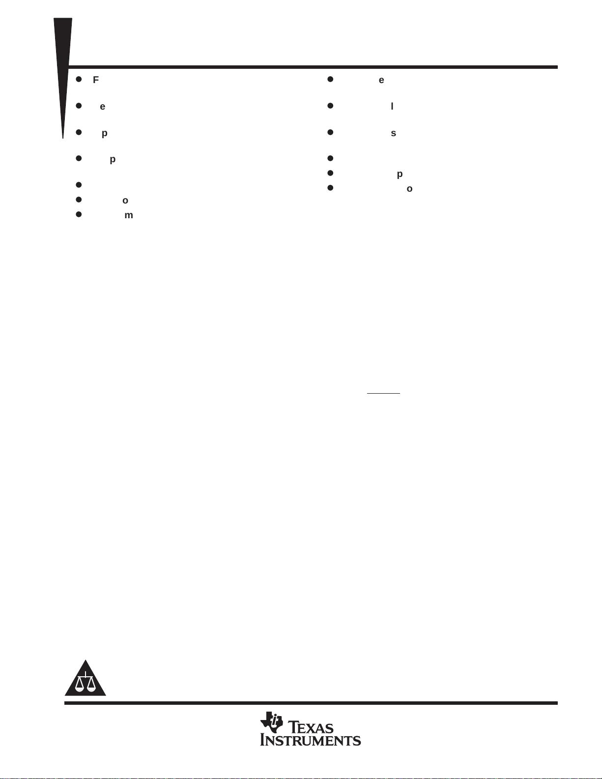
Package Options Include 44-Pin Plastic
Leaded Chip Carrier (FN) and 64-Pin Thin
Quad Flat (PAG, PM) Packages
description
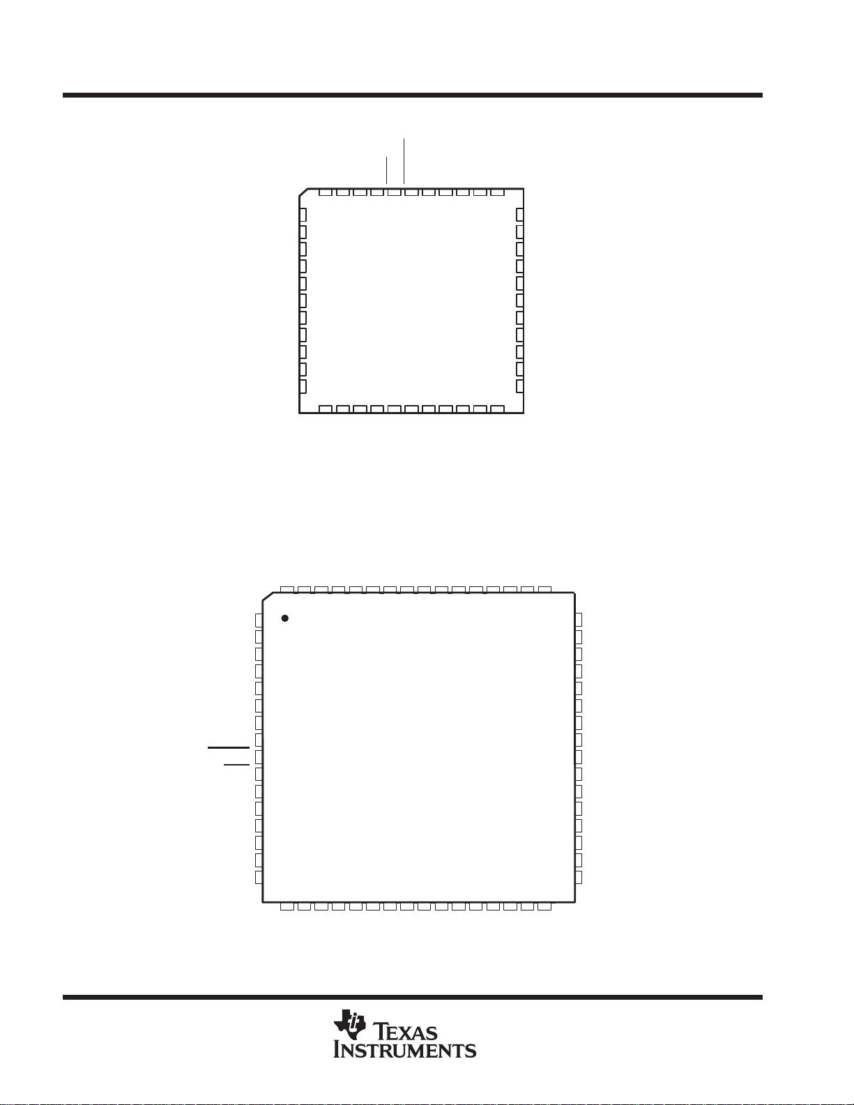
The SN74ACT7807 is a 2048-word by 9-bit FIFO with high speed and fast access times. It processes data at
rates up to 67 MHz and access times of 12 ns in a bit-parallel format. Data outputs are noninverting with respect
to the data inputs. Expansion is easily accomplished in both word width and word depth.
The write-clock (WRTCLK) and read-clock (RDCLK) inputs should be free running and can be asynchronous
or coincident. Data is written to memory on the rising edge of WRTCLK when the write-enable (WRTEN1/DP9,
WRTEN2) inputs are high and the input-ready (IR) flag output is high. Data is read from memory on the rising
edge of RDCLK when the read-enable (RDEN1, RDEN2) and output-enable (OE) inputs are high and the
output-ready (OR) flag output is high. The first word written to memory is clocked through to the output buffer
regardless of the levels on RDEN1, RDEN2, and OE. The OR flag indicates that valid data is present on the
output buffer.
The FIFO can be reset asynchronous to WRTCLK and RDCLK. RESET
must be asserted while at least four
WRTCLK and four RDCLK cycles occur to clear the synchronizing registers. Resetting the FIFO initializes the
IR, OR, and half-full (HF) flags low and the almost-full/almost-empty (AF/AE) flag high. The FIFO must be reset
upon power up.
The SN74ACT7807 is characterized for operation from 0°C to 70°C.
Copyright 1998, Texas Instruments Incorporated
PRODUCTION DATA information is current as of publication date.
Products conform to specifications per the terms of Texas Instruments
standard warranty. Production processing does not necessarily include
testing of all parameters.
Please be aware that an important notice concerning availability, standard warranty, and use in critical applications of
Texas Instruments semiconductor products and disclaimers thereto appears at the end of this data sheet.
剩余14页未读,继续阅读
资源评论


