TI-SN74ACT2235-60FN.pdf

需积分: 0 178 浏览量
更新于2022-12-11
5
收藏 248KB PDF 举报
TI-SN74ACT2235是一款高性能的异步双向FIFO(First-In, First-Out)内存芯片,主要用于高速数据传输和独立的数据写入与读取操作。该芯片采用低功耗的先进CMOS技术制造,具备双1024位×9位的数据存储能力,能够提供快速的存取时间。
这款FIFO内存的独特之处在于其独立的异步输入和输出,这意味着写入和读取操作可以在不同的速度下独立进行,这对于处理不同速率的数据流非常有用。它还配备了可编程的“几乎满”/“几乎空”标志,以及空、满和半满标志,这些标志能帮助用户监控内存的状态,以便于实现高效的数据管理和同步。
SN74ACT2235具有25纳秒的存取时间,即使在50皮法负载条件下,也能达到25纳秒的访问速度,支持高达50MHz的数据速率,这使得它在高速数据处理应用中表现出色。此外,它还具备最长达22纳秒的最大下降时间,确保了数据传输的及时性。
该器件还设计有高输出驱动能力,适合直接与总线接口,提供了44引脚塑封引脚芯片载体(FN)和64引脚薄型四边扁平封装(PAG, PM)等不同的封装选项,以适应不同的应用场景需求。
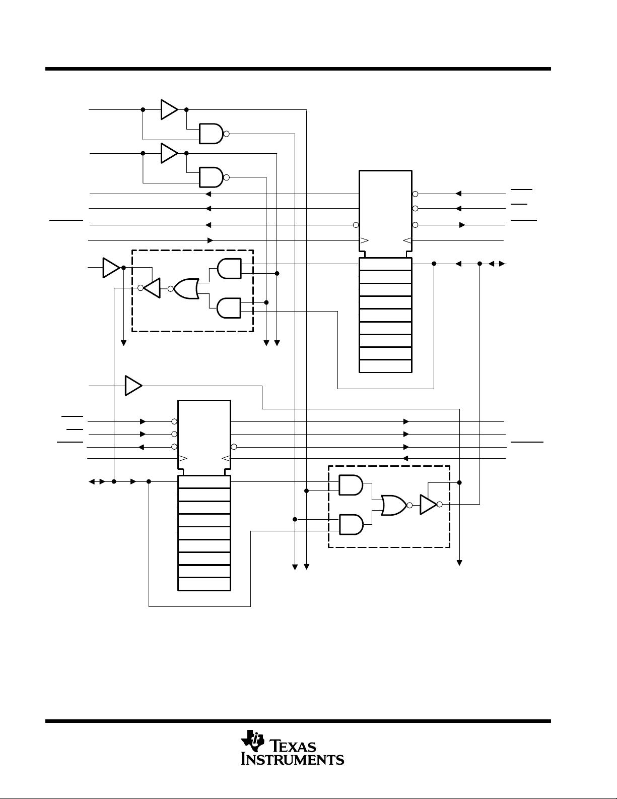
SN74ACT2235的内部结构包括总线转换器电路、两个1024位×9位的FIFO和控制电路。通过启用(GAB和GBA)输入可以控制转换器功能,而选择控制(SAB和SBA)输入则用于选择是实时传输数据还是从内部FIFO内存传输。这种选择控制电路消除了在存储数据和实时数据之间转换时通常出现的解码毛刺问题,提高了系统性能。
如图2所示,SN74ACT2235能够执行八种基本的总线管理功能,这使得它在各种复杂的系统环境中都能灵活地处理数据传输。为了获取更多关于该设备家族的信息,可以参考应用报告《1K × 9 × 2 Asynchronous FIFO SN74ACT2235》,文献编号SCAA010。
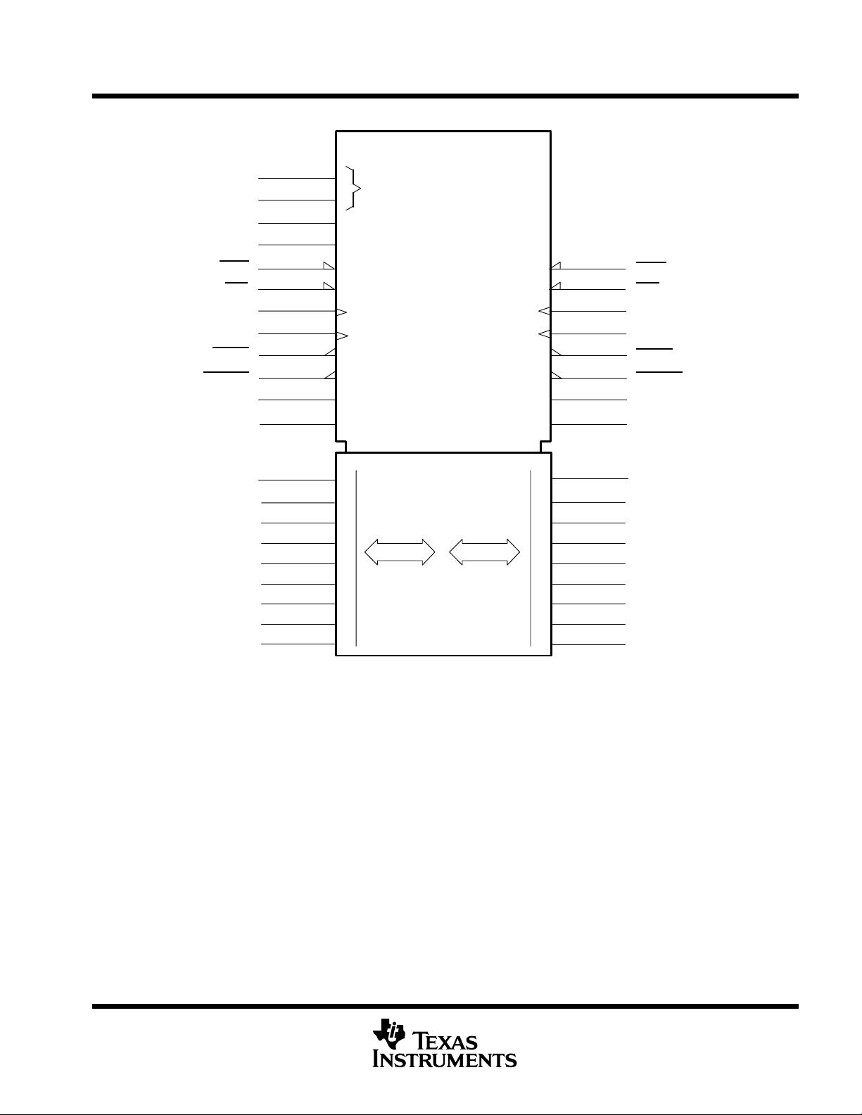
SN74ACT2235被规定在0°C至70°C的温度范围内工作,确保了其在广泛环境条件下的稳定性。该芯片的引脚布局包括VCC电源引脚、接地引脚(GND)、数据输入输出引脚(A0到A8和B0到B8)、控制信号引脚(如GAB、GNDB、AF/AE、LDA、CK等),以及状态标志引脚(如EMPTY、FULL等)。
TI-SN74ACT2235是一种高性能、低功耗的异步FIFO内存解决方案,适用于需要高速、高容量数据缓冲的应用,如通信、数据处理和工业自动化等领域。其强大的功能集、灵活的封装选项和广泛的温度操作范围使其成为许多现代电子系统设计的理想选择。
SN74ACT2235
1024 × 9 × 2
ASYNCHRONOUS BIDIRECTIONAL FIRST-IN, FIRST-OUT MEMORY
SCAS148F – DECEMBER 1990 – REVISED JUNE 2003
1
POST OFFICE BOX 655303 • DALLAS, TEXAS 75265
D
Independent Asynchronous Inputs and
Outputs
D
Low-Power Advanced CMOS Technology
D
Bidirectional
D
Dual 1024 by 9 Bits
D
Programmable Almost-Full/Almost-Empty
Flag
D
Empty, Full, and Half-Full Flags
D
Access Times of 25 ns With a 50-pF Load
D
Data Rates up to 50 MHz
D
Fall-Through Times of 22 ns Maximum
D
High Output Drive for Direct Bus Interface
D
Package Options Include 44-Pin Plastic
Leaded Chip Carriers (FN) and 64-Pin Thin
Quad Flat (PAG, PM) Packages
description
A FIFO memory is a storage device that allows data to be written into and read from its array at independent
data rates. The SN74ACT2235 is arranged as two 1024 × 9-bit FIFOs for high speed and fast access times.
It processes data at rates up to 50 MHz, with access times of 25 ns in a bit-parallel format.
The SN74ACT2235 consists of bus-transceiver circuits, two 1024 × 9-bit FIFOs, and control circuitry arranged
for multiplexed transmission of data directly from the data bus or from the internal FIFO memories. Enable (GAB
and GBA) inputs are provided to control the transceiver functions. The select-control (SAB and SBA) inputs are
provided to select whether real-time or stored data is transferred. The circuitry used for select control eliminates
the typical decoding glitch that occurs in a multiplexer during the transition between stored and real-time data.
Figure 2 shows the eight fundamental bus-management functions that can be performed with the
SN74ACT2235.
For more information on this device family, see the application report, 1K × 9 × 2 Asynchronous FIFO
SN74ACT2235, literature number SCAA010.
The SN74ACT2235 is characterized for operation from 0°C to 70°C.
B2
B3
B4
V
CC
B5
B6
B7
B8
GND
AF/AEB
HFB
39
38
37
36
35
34
33
32
31
30
29
18 19
7
8
9
10
11
12
13
14
15
16
17
A3
A4
V
CC
A5
A6
A7
A8
GND
AF/AEA
HFA
LDCKA
20 21 22 23
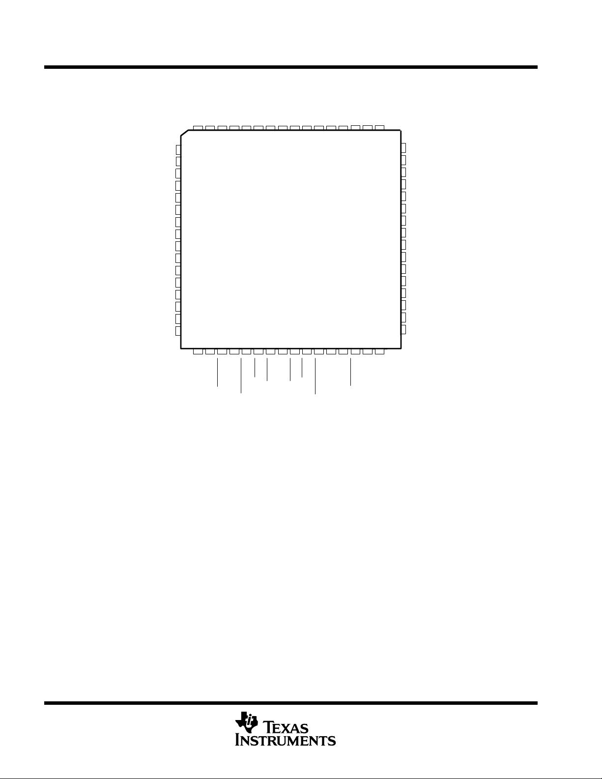
FN PACKAGE
(TOP VIEW)
GAB
GND
B0
B1
543 21644
A2
A1
A0
GND
GBA
SBA
SAB
EMPTYA
UNCKA
FULLB
LDCKB
FULLA
UNCKB
EMPTYB
DAF
RSTA
RSTB
DBF
42 41 4043
24 25 26 27 28
Copyright 2003, Texas Instruments Incorporated
PRODUCTION DATA information is current as of publication date.
Products conform to specifications per the terms of Texas Instruments
standard warranty. Production processing does not necessarily include
testing of all parameters.
Please be aware that an important notice concerning availability, standard warranty, and use in critical applications of
Texas Instruments semiconductor products and disclaimers thereto appears at the end of this data sheet.
剩余17页未读,继续阅读
资源评论


不觉明了
- 粉丝: 7423
- 资源: 5764


最新资源
- 基于微信小程序图书馆座位再利用系统-微信小程序毕业项目,适合计算机毕-设、实训项目、大作业学习.zip
- 基于微信小程序校园订餐的设计与开发+ssm-微信小程序毕业项目,适合计算机毕-设、实训项目、大作业学习.rar
- 基于微信小程序的科创微应用平台设计与实现+ssm-微信小程序毕业项目,适合计算机毕-设、实训项目、大作业学习.rar
- Python 实现粒子群优化(PSO)算法的深度置信网络(DBN)进行多输入单输出回归预测的实例(含完整的程序,GUI设计和代码详解)
- 基于小程序的物流管理系统---论文-微信小程序毕业项目,适合计算机毕-设、实训项目、大作业学习.zip
- 基于小程序的购物系统设计与实现+ssm-微信小程序毕业项目,适合计算机毕-设、实训项目、大作业学习.rar
- 基于微信小程序的教学质量评价系统ssm-微信小程序毕业项目,适合计算机毕-设、实训项目、大作业学习.rar
- Python 实现贝叶斯优化卷积神经网络(BO-CNN)进行时间序列预测的详细项目实例(含完整的程序,GUI设计和代码详解)
- 基于小程序的老孙电子点菜系统开发设计与实现+ssm-微信小程序毕业项目,适合计算机毕-设、实训项目、大作业学习.rar
- 基于微信小程序的社区垃圾回收管理系统ssm-微信小程序毕业项目,适合计算机毕-设、实训项目、大作业学习.rar
- Python 项目实例,展示如何使用LSTM(长短期记忆)神经网络进行时间序列预测(含完整的程序,GUI设计和代码详解)
- 基于微信小程序的企业职工薪资查询系统设计与实现+ssm-微信小程序毕业项目,适合计算机毕-设、实训项目、大作业学习.rar
- 基于微信小程序的商品展示+ssm-微信小程序毕业项目,适合计算机毕-设、实训项目、大作业学习.rar
- 基于智能推荐的校园社区服务微信小程序_5x8ot-微信小程序毕业项目,适合计算机毕-设、实训项目、大作业学习.zip
- 基于微信小程序的体育课评分系统+ssm-微信小程序毕业项目,适合计算机毕-设、实训项目、大作业学习.rar
- Python 实现BO-CNN(贝叶斯优化卷积神经网络)模型的详细项目实例(含完整的程序,GUI设计和代码详解)
