TI-SN74LV8154-EP.pdf
需积分: 5 95 浏览量
2022-11-29
12:53:52
上传
评论 4
收藏 807KB PDF 举报

SCLS704A − JULY 2006 − REVISED SEPTEMBER 2007
1
POST OFFICE BOX 655303 • DALLAS, TEXAS 75265
D Controlled Baseline
− One Assembly Site
− One Test Site
− One Fabrication Site
D Extended Temperature Performance of
−55°C to 125°C
D Enhanced Diminishing Manufacturing
Sources (DMS) Support
D Enhanced Product-Change Notification
D Qualification Pedigree
†
D Can Be Used as Two 16 Bit Counters or a
Single 32 Bit Counter
D 2-V to 5.5-V V
CC
Operation
D Max t
pd
of 25 ns at 5 V (RCLK to Y)
D Typical V
OLP
(Output Ground Bounce)
<0.7 V at V
CC
= 5 V, T
A
= 25°C
D Typical V
OHV
(Output V
OH
Undershoot)
>4.4 V at V
CC
= 5 V, T
A
= 25°C
D I
off
Supports Partial-Power-Down Mode
Operation
D Latch-Up Performance Exceeds 250 mA Per
JESD 17
D ESD Protection Exceeds JESD 22
− 2000-V Human-Body Model (A114-A)
− 200-V Machine Model (A115-A)
− 1000-V Charged-Device Model (C101)
†
Component qualification in accordance with JEDEC and industry
standards to ensure reliable operation over an extended
temperature range. This includes, but is not limited to, Highly
Accelerated Stress Test (HAST) or biased 85/85, temperature
cycle, autoclave or unbiased HAST, electromigration, bond
intermetallic life, and mold compound life. Such qualification
testing should not be viewed as justifying use of this component
beyond specified performance and environmental limits.
description/ordering information
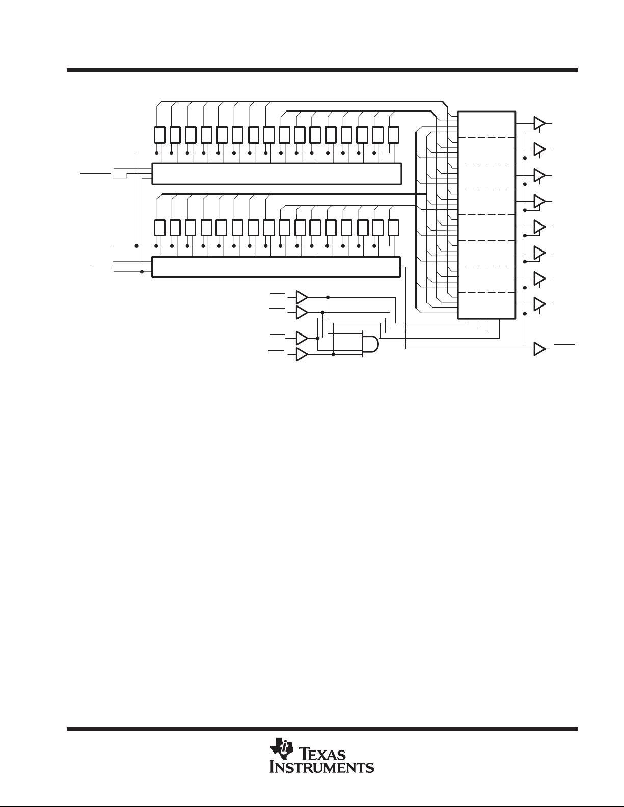
The SN74LV8154 is a dual 16 bit binary counter with 3-state output registers, designed for 2-V to 5.5-V V
CC
operation.
This 16 bit counter (A or B) feeds a 16 bit storage register and each storage register is further divided into an
upper byte and lower byte. The GAL
, GAU, GBL, and GBU inputs are used to select the byte that needs to be
output at Y0−Y7. CLKA is the clock for A counter and CLKB is the clock for B counter. RCLK is the clock for the
A and B storage registers. All three clock signals are positive-edge triggered.
A 32 bit counter can be realized by connecting CLKA and CLKB together and by connecting RCOA
to CLKBEN.
To ensure the high-impedance state during power up or power down, GAL
, GAU, GBL, and GBU should be tied
to V
CC
through a pullup resistor; the minimum value of the resistor is determined by the current-sinking capability
of the driver.
This device is fully specified for partial-power-down applications using I
off
. The I
off
circuitry disables the outputs,
preventing damaging current backflow through the device when it is powered down.
ORDERING INFORMATION
†
T
A
PACKAGE
}
ORDERABLE
PART NUMBER
TOP-SIDE
MARKING
−55°C to 125°C TSSOP − PW Tape and reel SN74LV8154MPWREP LV8154ME
†
For the most current package and ordering information, see the Package Option Addendum at the
end of this document, or see the TI website at www.ti.com.
‡
Package drawings, standard packing quantities, thermal data, symbolization, and PCB design
guidelines are available at www.ti.com/packaging.
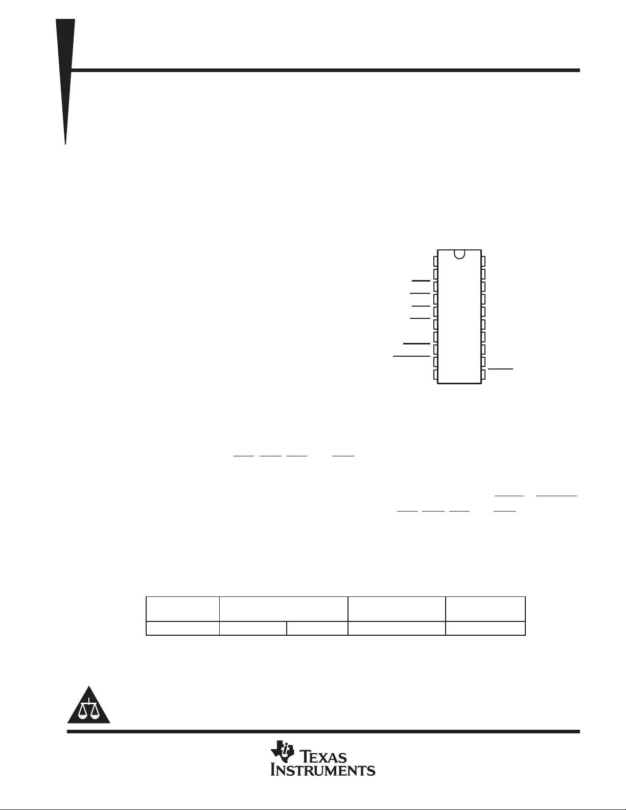
PW PACKAGE
(TOP VIEW)
CLKA
CLKB
GAL
GAU
GBL
GBU
RCLK
RCOA
CLKBEN
GND
V
CC
Y0
Y1
Y2
Y3
Y4
Y5
Y6
Y7
CCLR
1
2
3
4
5
6
7
8
9
10
20
19
18
17
16
15
14
13
12
11
Copyright 2007, Texas Instruments Incorporated
Please be aware that an important notice concerning availability, standard warranty, and use in critical applications o
f
Texas Instruments semiconductor products and disclaimers thereto appears at the end of this data sheet.
!"#$ % &'!!($ #% )'*+&#$ ,#$(-
!,'&$% &!" $ %)(&&#$% )(! $.( $(!"% (/#% %$!'"($%
%$#,#!, 0#!!#$1- !,'&$ )!&(%%2 ,(% $ (&(%%#!+1 &+',(
$(%$2 #++ )#!#"($(!%-

剩余14页未读,继续阅读
资源评论


