TI-TPL0102-EP.pdf
需积分: 10 143 浏览量
2022-11-27
16:35:47
上传
评论 4
收藏 1.13MB PDF 举报

I
2
C INTERFACE
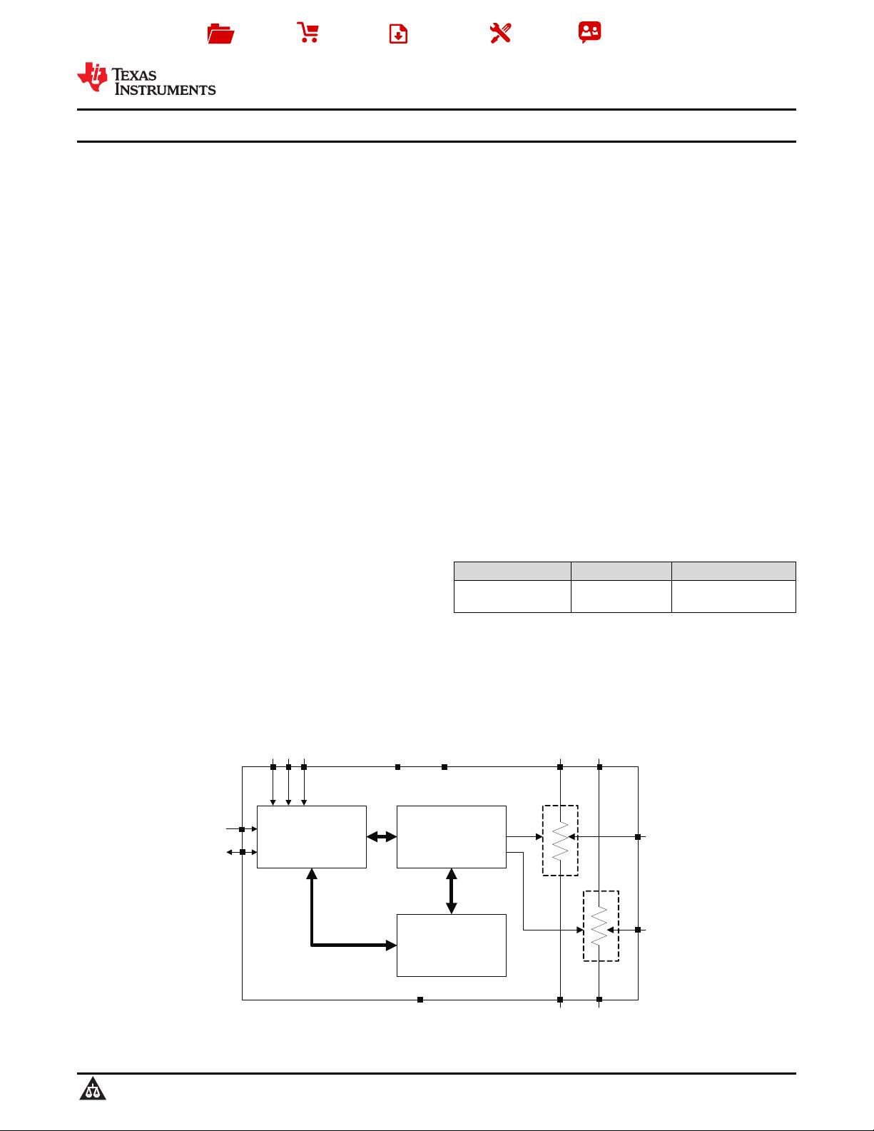
VOLATILE
REGISTERS
NON-VOLATILE
REGISTERS
A0 A1 A2 HA
LA
HB
LB
WA
WB
VDD VSS
GND
SDA
SCL
Product
Folder
Sample &
Buy
Technical
Documents
Tools &
Software
Support &
Community
TPL0102-EP
SLIS149 –JUNE 2014
TPL0102-EP 256-Taps Dual-Channel Digital Potentiometer With Non-Volatile Memory
1 Features 2 Applications
1
• Dual-Channel, 256-Position Resolution
• Adjustable Gain Amplifiers and Offset Trimming
• Non-Volatile Memory Stores Wiper Settings • Adjustable Power Supplies
• 2-mm × 2-mm, 14-Pin TSSOP Package • Precision Calibration of Set Point Thresholds
• 100-kΩ End-to-End Resistance (TPL0102-100) • Sensor Trimming and Calibration
• Fast Power-Up Response Time to Wiper Setting: • Mechanical Potentiometer Replacement
<100 µs
3 Description
• ±0.5 LSB INL, ±0.25 LSB DNL (Voltage-Divider
The TPL0102-EP is a two-channel, linear-taper digital
Mode)
potentiometer with 256 wiper positions. Each
• 4 ppm/°C Ratiometric Temperature Coefficient
potentiometer can be used as a three-terminal
• I
2
C-Compatible Serial Interface
potentiometer or as a two-terminal rheostat. The
• 2.7- to 5.5-V Single-Supply Operation
TPL0102-EP-100 has an end-to-end resistance of
100 kΩ.
• ±2.25 to ±2.75 V Dual-Supply Operation
The TPL0102-EP has non-volatile memory
• Operating Temperature Range From
(EEPROM) which can be used to store the wiper
–40°C to 125°C
position. The internal registers of the TPL0102-EP
• ESD Performance Tested Per JESD 22
can be accessed using the I
2
C interface.
– 2000-V Human Body Model
The TPL0102-EP is available in a 14-pin TSSOP
(A114-B, Class II)
package with a specified temperature range of –40°C
• Supports Defense, Aerospace, and Medical
to 125°C.
Applications
– Controlled Baseline
Device Information
(1)
ORDER NUMBER PACKAGE BODY SIZE (NOM)
– One Assembly and Test Site
TPL0102-
– One Fabrication Site
TSSOP (14) 5.00 mm × 4.40 mm
100QPWREP
– Available in Extended (Q) Temperature –40°C
(1) For all available packages, see the orderable addendum at
to 125°C
the end of the data sheet.
– Extended Product Life Cycle
– Extended Product-Change Notification
– Product Traceability
4 Functional Block Diagram
1
An IMPORTANT NOTICE at the end of this data sheet addresses availability, warranty, changes, use in safety-critical applications,
intellectual property matters and other important disclaimers. PRODUCTION DATA.


剩余35页未读,继续阅读
资源评论


不觉明了
- 粉丝: 3164
- 资源: 5429


最新资源
- 基于matlab实现本份代码能对图像进行gabor滤波处理,结合指纹方向图以及指纹沟壑频率特性,对指纹图像进行增强.rar
- 基于matlab实现RBM神经网络实现了手写数字体识别的GUI程序.rar
- 基于matlab实现蝙蝠算法优化相关向量机建模对数据进行建模和预测.rar
- 基于matlab实现编写的禁忌搜索算法,解决了TSP问题,对初学者有重要的参考价值.rar
- 基于matlab实现SOH关于IMU进行姿态求解的C代码,里面包含了两套代码,分别是重力约束法求解和梯度下降法求解.rar
- 1_简单电子邮件客户端.zip
- 基于matlab实现powell优化搜索算法,适合于多参数优化且目标函数中不包含参数的情况.rar
- 基于matlab实现PID神经网络前向和反向学习算法的matlab的原程序代码.rar
- 基于matlab实现nsga-2的多目标优化算法,有注解.rar
- AIR-AP1815-K9-ME-8-5-182-0.zipFor 1815 1830 1840 1850 2700 3700
资源上传下载、课程学习等过程中有任何疑问或建议,欢迎提出宝贵意见哦~我们会及时处理!
点击此处反馈


