没有合适的资源?快使用搜索试试~ 我知道了~
TI-SN74GTL2014.pdf
需积分: 9 0 下载量 11 浏览量
2022-11-30
23:10:39
上传
评论 4
收藏 1.09MB PDF 举报
温馨提示
![preview](https://dl-preview.csdnimg.cn/87222329/0001-b848ceab24e3285044c64d3399fbf30f_thumbnail.jpeg)
![preview-icon](https://csdnimg.cn/release/downloadcmsfe/public/img/scale.ab9e0183.png)
试读
19页
TI-SN74GTL2014.pdf
资源推荐
资源详情
资源评论
![application/x-rar](https://img-home.csdnimg.cn/images/20210720083606.png)
![](https://csdnimg.cn/release/download_crawler_static/87222329/bg1.jpg)
+
–
GTL2014
B0
B1
B2
B3
VREF
DIR
002aab139
A3
A2
A1
A0
+
–
+
–
+
–
Product
Folder
Sample &
Buy
Technical
Documents
Tools &
Software
Support &
Community
SN74GTL2014
ZHCSCJ4A –FEBRUARY 2014–REVISED OCTOBER 2014
SN74GTL2014 4 通通道道 LVTTL 至至 GTL 收收发发器器
1 特特性性 2 应应用用
1
• 可用作 GTL–/GTL/GTL+ 至 LVTTL 转换器或
• 服务器
LVTTL 至 GTL–/GTL/GTL+ 转换器
• 基站
• LVTTL 输入最高可承受 5.5V 电压,允许直接访问
• 有线通信
TTL 或 5V CMOS
3 说说明明
• GTL 输入/输出工作电压高达 3.6V,这使得器件可
在高压开漏应用中使用
SN74GTL2014 是一款 4 通道转换器,用于连接 3.3V
• VREF 可降至 0.5V,以实现低电压 CPU 使用率
LVTTL 芯片组 I/O 与 Xeon 处理器 GTL–/GTL/GTL+
• 支持局部断电
I/O。
• 锁断保护超过 500mA,符合 JESD78 规范的要求
SN74GTL2014 在所有端子上集成了 ESD 保护单元,
• 封装选项:TSSOP14
并且采用 TSSOP 封装 (5.0mm × 4.4mm)。 器件在自
• -40°C 至 + 85°C 工作温度范围
然通风环境下的额定工作温度范围为 -40°C 至 85°C。
• 所有端子上具备静电放电 (ESD) 保护
– 2000V 人体模型 (HBM),JESD22-A114
器器件件信信息息
(1)
– 1000V 充电器件模型 (CDM),IEC61000-4-2
部部件件号号 封封装装 封封装装尺尺寸寸((标标称称值值))
薄型小外形尺寸封装
SN74GTL2014 5.00mm x 4.40mm
(TSSOP) (14)
(1) 要了解所有可用封装,请见数据表末尾的可订购产品附录。
1
PRODUCTION DATA information is current as of publication date. Products conform to specifications per the terms of the Texas
Instruments standard warranty. Production processing does not necessarily include testing of all parameters.
English Data Sheet: SCLS746
![](https://csdnimg.cn/release/download_crawler_static/87222329/bg2.jpg)
SN74GTL2014
ZHCSCJ4A –FEBRUARY 2014–REVISED OCTOBER 2014
www.ti.com.cn
目目录录
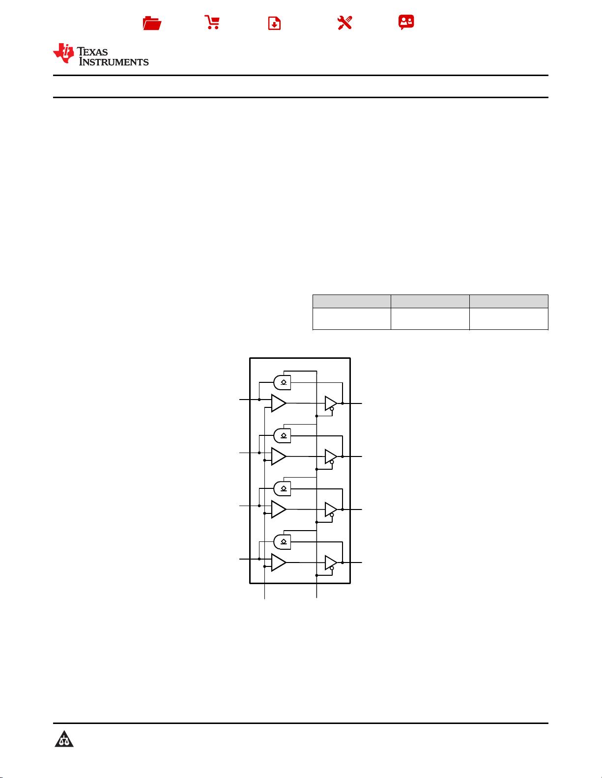
8.2 Functional Block Diagram ......................................... 8
1 特特性性.......................................................................... 1
8.3 Feature Description................................................... 8
2 应应用用.......................................................................... 1
8.4 Device Functional Modes.......................................... 8
3 说说明明.......................................................................... 1
9 Application and Implementation .......................... 9
4 修修订订历历史史记记录录 ........................................................... 2
9.1 Application Information.............................................. 9
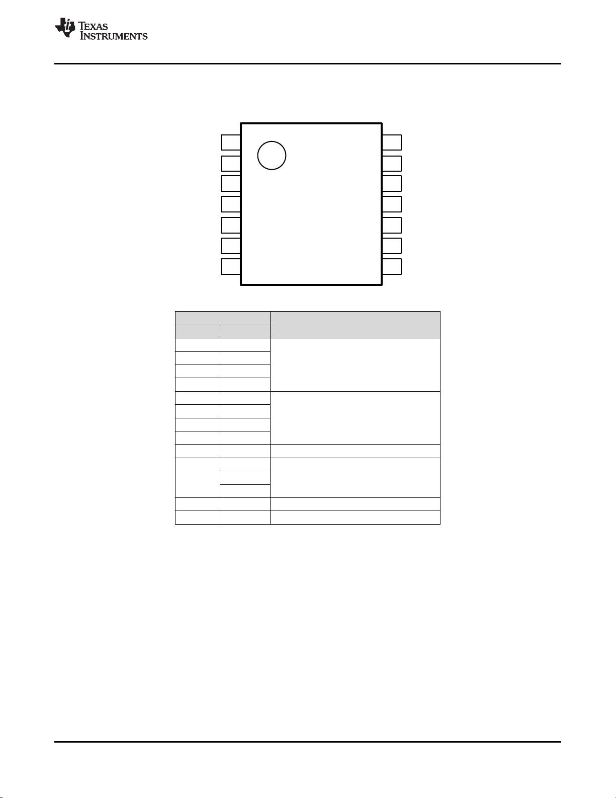
5 Pin Configuration and Functions......................... 3
9.2 Typical Application .................................................... 9
6 Specifications......................................................... 4
10 Power Supply Recommendations ..................... 12
6.1 Absolute Maximum Ratings ...................................... 4
11 Layout................................................................... 12
6.2 Handling Ratings....................................................... 4
11.1 Layout Guidelines ................................................. 12
6.3 Recommended Operating Conditions....................... 4
11.2 Layout Example .................................................... 12
6.4 Thermal Information.................................................. 5
12 器器件件和和文文档档支支持持 ..................................................... 13
6.5 Electrical Characteristics........................................... 5
12.1 商标 ....................................................................... 13
6.6 Dynamic Electrical Characteristics............................ 6
12.2 静电放电警告......................................................... 13
6.7 Typical Characteristics.............................................. 6
12.3 术语表 ................................................................... 13
7 Parameter Measurement Information .................. 7
13 机机械械封封装装和和可可订订购购信信息息 .......................................... 13
8 Detailed Description .............................................. 8
8.1 Overview ................................................................... 8
4 修修订订历历史史记记录录
Changes from Original (February 2014) to Revision A Page
• 已添加 添加了处理额定值表,特性描述部分,器件功能模式,应用和实施部分,电源相关建议部分,布局部分,器件
和文档支持部分以及机械、封装和可订购信息部分。 ............................................................................................................ 1
• Updated Specifications section .............................................................................................................................................. 4
• Updated LVTTL/TTL to GTL–/GTL/GTL+ application schematic. ......................................................................................... 9
• Updated LVTTL/TTL to GTL–/GTL/GTL+ application schematic. ....................................................................................... 11
• Added Power Supply Recommendations ............................................................................................................................ 12
2 Copyright © 2014, Texas Instruments Incorporated
![](https://csdnimg.cn/release/download_crawler_static/87222329/bg3.jpg)
GTL2014
DIR
B0
B1
VREF
B2
GND
VCC
A0
A1
GND
A2
A3
GND
1
2
3
4
5
6
7
8
9
10
11
12
13
14
B3
SN74GTL2014
www.ti.com.cn
ZHCSCJ4A –FEBRUARY 2014–REVISED OCTOBER 2014
5 Pin Configuration and Functions
TSSOP Package (14 Pin)
(Top View)
Pin Functions
PIN
DESCRIPTION
NAME NUMBER
A0 13
A01 12
LVTTL data input/output
A02 10
A03 9
B0 2
B01 3
GTL data input/output
B02 5
B03 6
DIR 1 Direction control input (LVTTL)
7
GND 8 Ground
11
VCC 14 Supply voltage
VREF 4 GTL reference voltage
Copyright © 2014, Texas Instruments Incorporated 3
![](https://csdnimg.cn/release/download_crawler_static/87222329/bg4.jpg)
SN74GTL2014
ZHCSCJ4A –FEBRUARY 2014–REVISED OCTOBER 2014
www.ti.com.cn
6 Specifications
6.1 Absolute Maximum Ratings
Specified at T
A
= –40°C to 85°C unless otherwise noted
(1)
MIN MAX UNIT
V
CC
Supply voltage –0.5 4.6 V
I
IK
Input clamping current, VI < 0 V –50 mA
V
SEL
Input control voltages SEL
(2)(3)
–0.5 6 V
A port –0.5 7
V
I
Input voltage V
B port –0.5 4.6
I
OK
Control input clamp current, V
O
< 0 V –50 mA
A port –0.5 7
V
O
Output voltage V
B port –0.5 4.6
A port 40
I
OL
Current into any output in the low state mA
B port 80
I
OH
Current into any output in the high state –40 mA
(1) Stresses beyond those listed under Absolute Maximum Ratings may cause permanent damage to the device. These are stress ratings
only and functional operation of the device at these conditions is not implied. Exposure to absolute-maximum-rated conditions for
extended periods may affect device reliability.
(2) All voltages are with respect to ground, unless otherwise specified
(3) V
I
and V
O
are used to denote specific conditions for V
I/O
6.2 Handling Ratings
MIN MAX UNIT
T
stg
Storage temperature range –55 150 °C
Human Body Model (HBM), JEDEC: JESD22-A114
(2)
All pins 0 2
V
ESD
(1)
kV
IEC61000-4-2 contact discharge
(3)
All pins 0 1
(1) Electrostatic discharge (ESD) to measure device sensitivity/immunity to damage caused by assembly line electrostatic discharges into
the device.
(2) Level listed above is the passing level per ANSI/ESDA/JEDEC JS-001. JEDEC document JEP155 states that 500-V HBM allows safe
manufacturing with a standard ESD control process. Pins listed as 250 V may actually have higher performance.
(3) Level listed above is the passing level per EIA-JEDEC JESD22-C101. JEDEC document JEP157 states that 250-V CDM allows safe
manufacturing with a standard ESD control process. Pins listed as 250 V may actually have higher performance.
6.3 Recommended Operating Conditions
over operating free-air temperature range (unless otherwise noted)
(1)
MIN NOM MAX UNIT
V
CC
Supply voltage 3 3.3 3.6 V
GTL– 0.85 0.9 0.95
V
TT
Termination voltage GTL 1.14 1.2 1.26 V
GTL+ 1.35 1.5 1.65
Overall 0.5 2 / 3 V
TT
V
CC
/ 2
GTL– 0.5 0.6 0.63
V
REF
Reference voltage V
GTL 0.76 0.8 0.84
GTL+ 0.87 1 1.1
A port 0 3.3 5.5
(2)
V
I
Input voltage V
B port 0 V
TT
3.6
A port and DIR 2
V
IH
High-level input voltage V
B port V
REF
+ 50 mV
(1) All unused control inputs of the device must be held at V
CC
or GND to ensure proper device operation. Refer to the TI application report,
Implications of Slow or Floating CMOS Inputs, literature number SCBA004.
(2) The V
I(max
) of LVTTL port is 3.6 V if configured as output (DIR=L)
4 Copyright © 2014, Texas Instruments Incorporated
剩余18页未读,继续阅读
资源评论
![avatar-default](https://csdnimg.cn/release/downloadcmsfe/public/img/lazyLogo2.1882d7f4.png)
![avatar](https://profile-avatar.csdnimg.cn/107303f5121d47e49d12d0a9ae68af10_weixin_54787054.jpg!1)
不觉明了
- 粉丝: 3236
- 资源: 5614
上传资源 快速赚钱
我的内容管理 展开
我的资源 快来上传第一个资源
我的收益
登录查看自己的收益我的积分 登录查看自己的积分
我的C币 登录后查看C币余额
我的收藏
我的下载
下载帮助
![voice](https://csdnimg.cn/release/downloadcmsfe/public/img/voice.245cc511.png)
![center-task](https://csdnimg.cn/release/downloadcmsfe/public/img/center-task.c2eda91a.png)
安全验证
文档复制为VIP权益,开通VIP直接复制
![dialog-icon](https://csdnimg.cn/release/downloadcmsfe/public/img/green-success.6a4acb44.png)