没有合适的资源?快使用搜索试试~ 我知道了~
TI-SN74F1016.pdf
需积分: 10 0 下载量 165 浏览量
2022-11-29
23:11:42
上传
评论 4
收藏 990KB PDF 举报
温馨提示
试读
12页
TI-SN74F1016.pdf
资源推荐
资源详情
资源评论
SDFS093 − NOVEMBER 1992 − REVISED DECEMBER 1993
Copyright 1993, Texas Instruments Incorporated
2−1
POST OFFICE BOX 655303 • DALLAS, TEXAS 75265
POST OFFICE BOX 1443 • HOUSTON, TEXAS 77251−1443
• Designed to Reduce Reflection Noise
• Repetitive Peak Forward
Current . . . 300 mA
• 16-Bit Array Structure Suited for
Bus-Oriented Systems
description
This bus-termination array is designed to reduce
reflection noise and minimize ringing on
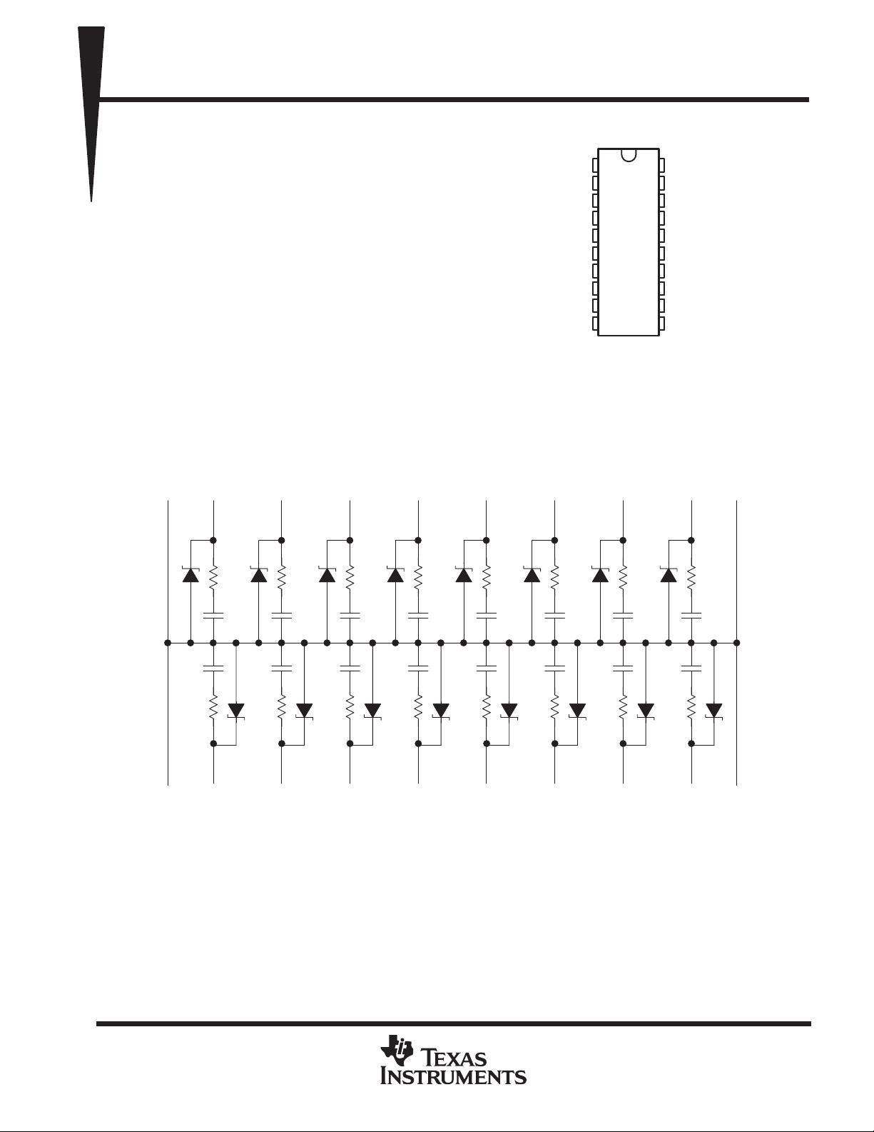
high-performance bus lines. The SN74F1016
features a 16-bit R-C network and Schottky barrier
diode array. These Schottky diodes provide
clamp-to-ground functionality and serve to
minimize overshoot and undershoot of
high-speed switching buses.
The SN74F1016 is characterized for operation
from 0°C to 70°C.
schematic diagram
20 19 18 17 16 15 14 13 12 11
12 3 4 5 6 7 8 910
GND A16 A15 A14 A13 A12 A11 A10 A9 GND
GND A1 A2 A3 A4 A5 A6 A7 A8 GND
Resistor = 50 Ω ± 10%
Capacitor = 47 pF ± 10%, V
R
= 2.5 V, f = 1 MHz
Diode = Schottky
DW PACKAGE
(TOP VIEW)
1
2
3
4
5
6
7
8
9
10
20
19
18
17
16
15
14
13
12
11
GND
A1
A2
A3
A4
A5
A6
A7
A8
GND
GND
A16
A15
A14
A13
A12
A11
A10
A9
GND
!" # $%&" !# '%()$!" *!"&+
*%$"# $ " #'&$$!"# '& ",& "&# &-!# #"%&"#
#"!*!* .!!"/+ *%$" '$&##0 *&# " &$&##!)/ $)%*&
"&#"0 !)) '!!&"&#+
SDFS093 − NOVEMBER 1992 − REVISED DECEMBER 1993
2−2
POST OFFICE BOX 655303 • DALLAS, TEXAS 75265
POST OFFICE BOX 1443
• HOUSTON, TEXAS 77251−1443
absolute maximum ratings over operating free-air temperature range (unless otherwise noted)
†
Steady-state reverse voltage, V
R
7 V. . . . . . . . . . . . . . . . . . . . . . . . . . . . . . . . . . . . . . . . . . . . . . . . . . . . . . . . . . . . .
Continuous forward current, I
F
: Any D terminal from GND 50 mA. . . . . . . . . . . . . . . . . . . . . . . . . . . . . . . . . . . .
Total through all GND terminals 170 mA. . . . . . . . . . . . . . . . . . . . . . . . . . . . . .
Repetitive peak forward current, I
FRM
‡
: Any D terminal from GND 300 mA. . . . . . . . . . . . . . . . . . . . . . . . . . . .
Total through all GND terminals 1.2 A. . . . . . . . . . . . . . . . . . . . . . . . .
Continuous total power dissipation at (or below) 25°C free-air temperature 500 mW. . . . . . . . . . . . . . . . . . . .
Operating free-air temperature range 0°C to 70°C. . . . . . . . . . . . . . . . . . . . . . . . . . . . . . . . . . . . . . . . . . . . . . . . . .
Storage temperature range −65°C to 150°C. . . . . . . . . . . . . . . . . . . . . . . . . . . . . . . . . . . . . . . . . . . . . . . . . . . . . . . .
†
Stresses beyond those listed under “absolute maximum ratings” may cause permanent damage to the device. These are stress ratings only and
functional operation of the device at these or any other conditions beyond those indicated under “recommended operating conditions” is not
implied. Exposure to absolute-maximum-rated conditions for extended periods may affect device reliability.
‡
These values apply for t
w
≤ 100 µs, duty cycle ≤ 20%.
electrical characteristics over recommended operating free-air temperature range (unless
otherwise noted)
single-diode operation (see Note 1)
PARAMETER TEST CONDITIONS MIN TYP
†
MAX UNIT
I
R
Static reverse current V
R
= 7 V 2 µA
V
FM
Peak forward voltage I
F
= 200 mA 1.25 V
V
R
= 0 80
C
t
Total capacitance
V
R
= 2 V
60
pF
C
t
Total capacitance
V
R
= 3 V 55
pF
†
All typical values are at T
A
= 25°C.
NOTE 1: Test conditions and limits apply separately to each of the diodes. The diodes not under test are open-circuited during the measurement
of these characteristics.
multiple-diode operation
PARAMETER TEST CONDITIONS MIN TYP
†
MAX UNIT
I
x
Internal crosstalk current Total GND current = 1.2 A, See Note 2 10 50 µA
NOTE 2: I
x
is measured under the following conditions with one diode static, all others switching:
Switching diodes: t
w
= 100 µs, duty cycle = 20%;
Static diode: V
R
= 5 V; the static diode input current is the internal crosstalk current I
x
.
switching characteristics, T
A
= 25°C
PARAMETER TEST CONDITIONS MIN TYP
†
MAX UNIT
t
rr
Reverse recovery time I
F
= 10 mA, I
RM(REC)
= 10 mA, I
R(REC)
= 1 mA, R
L
= 100 Ω 8 10 ns
undershoot characteristics
PARAMETER TEST CONDITIONS MIN TYP
†
MAX UNIT
V
US
Undershoot voltage
t
f
= 2 ns, t
w
= 50 ns, V
IH
= 5 V, V
IL
= 0, Z
S
= 25 Ω, Z
O
= 50 Ω,
L = 36-inch coaxial cable
0.7 0.8 V
SDFS093 − NOVEMBER 1992 − REVISED DECEMBER 1993
2−3
POST OFFICE BOX 655303 • DALLAS, TEXAS 75265
POST OFFICE BOX 1443
• HOUSTON, TEXAS 77251−1443
APPLICATION INFORMATION
Large negative transients occurring at the inputs of memory devices (DRAMs, SRAMs, EPROMs, etc.) or on the
CLOCK lines of many clocked devices can result in improper operation of the devices. The SN74F1016 diode
termination array helps suppress negative transients caused by transmission line reflections, crosstalk, and switching
noise.
Diode terminations have several advantages when compared to resistor termination schemes. Split resistor or
Thevenin equivalent termination can cause a substantial increase in power consumption. The use of a single resistor
to ground to terminate a line usually results in degradation of the output high level, resulting in reduced noise immunity.
Series damping resistors placed on the outputs of the driver will reduce negative transients, but they can also increase
propagation delays down the line, as a series resistor reduces the output drive capability of the driving device. Diode
terminations have none of these drawbacks.
The operation of the diode arrays in reducing negative transients is explained in Figure 1. The diode conducts current
whenever the voltage reaches a negative value large enough for the diode to turn on. Suppression of negative
transients is tracked by the current-voltage characteristic curve for that diode. A typical current voltage for the
SN74F1016 is shown in Figure 1.
The maximum effectiveness of the diode arrays in suppressing negative transients occurs when they are placed at
the end of a line and/or the end of a long stub branching off a main transmission line. The diodes can also be used
to reduce the negative transients that occur due to discontinuities in the middle of a line. An example of this is a slot
in a backplane that is provided for an add-on card.
0 0.2 0.4 0.6 0.8 1 1.2 1.4 1.6 1.8 2
− Forward Current − mA
V
F
− Forward Voltage − V
T
A
= 25°C
I
I
Variable 1:
V
IN
−Ch1
Linear Sweep:
Start 0.000 V
Stop −2.000 V
Step − 0.010 V
Constants:
V
HI
−Vs1 3.5000 V
V
LO
−Vs2 0.0000 V
−100
−90
−80
−70
−60
−50
−40
−30
−20
−10
0
DIODE FORWARD CURRENT
vs
DIODE FORWARD VOLTAGE
Figure 1
剩余11页未读,继续阅读
资源评论
不觉明了
- 粉丝: 3169
- 资源: 5430
上传资源 快速赚钱
- 我的内容管理 展开
- 我的资源 快来上传第一个资源
- 我的收益 登录查看自己的收益
- 我的积分 登录查看自己的积分
- 我的C币 登录后查看C币余额
- 我的收藏
- 我的下载
- 下载帮助
安全验证
文档复制为VIP权益,开通VIP直接复制
信息提交成功