SN74ALVC3631, SN74ALVC3641, SN74ALVC3651
512 × 36, 1024 × 36, 2048 × 36
SYNCHRONOUS FIRST-IN, FIRST-OUT MEMORIES
SDMS025B – OCTOBER 1999 – REVISED JUNE 2000
1
POST OFFICE BOX 655303 • DALLAS, TEXAS 75265
D
Free-Running CLKA and CLKB Can Be
Asynchronous or Coincident
D
Clocked FIFO Buffering Data From Port A
to Port B
D
Synchronous Read-Retransmit Capability
D
Mailbox Register in Each Direction
D
Programmable Almost-Full (AF) and
Almost-Empty (AE) Flags
D
Microprocessor Interface Control Logic
D
Input-Ready and AF Flags Synchronized by
CLKA
D
Output-Ready and AE Flags Synchronized
by CLKB
D
Low-Power 0.8-µm Advanced CMOS
Technology
D
Supports Clock Frequencies up to 100 MHz
D
Fast Access Times of 6.5 ns
D
Pin-to-Pin Compatible With 5-V Operating
SN74ACT3631, SN74ACT3641, and
SN74ACT3651
D
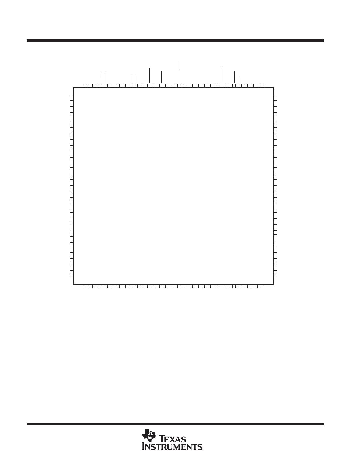
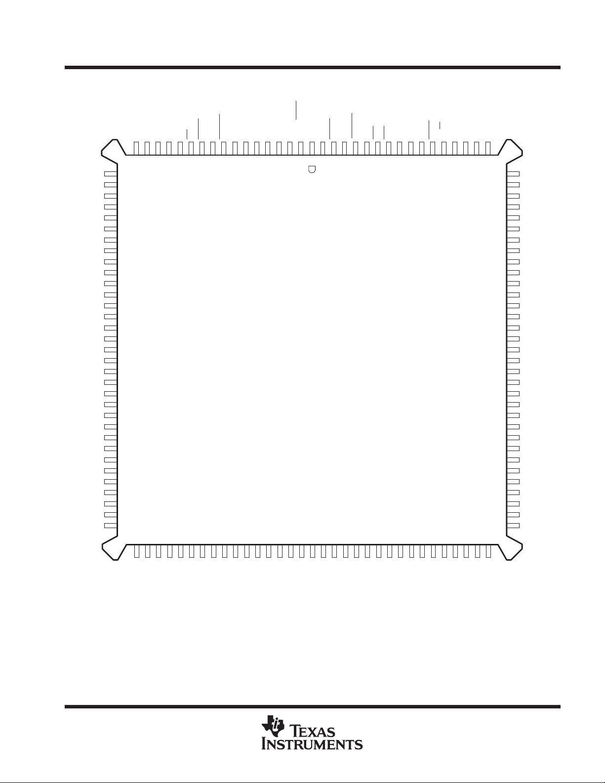
Package Options Include 120-Pin Thin
Quad Flat (PCB) and 132-Pin Plastic Quad
Flat (PQ) Packages
description
The SN74ALVC3631, SN74ALVC3641, and SN74ALVC3651 are high-speed, low-power, CMOS, synchronous
FIFO memories that support clock frequencies up to 100 MHz and have read access times as fast as 6.5 ns.
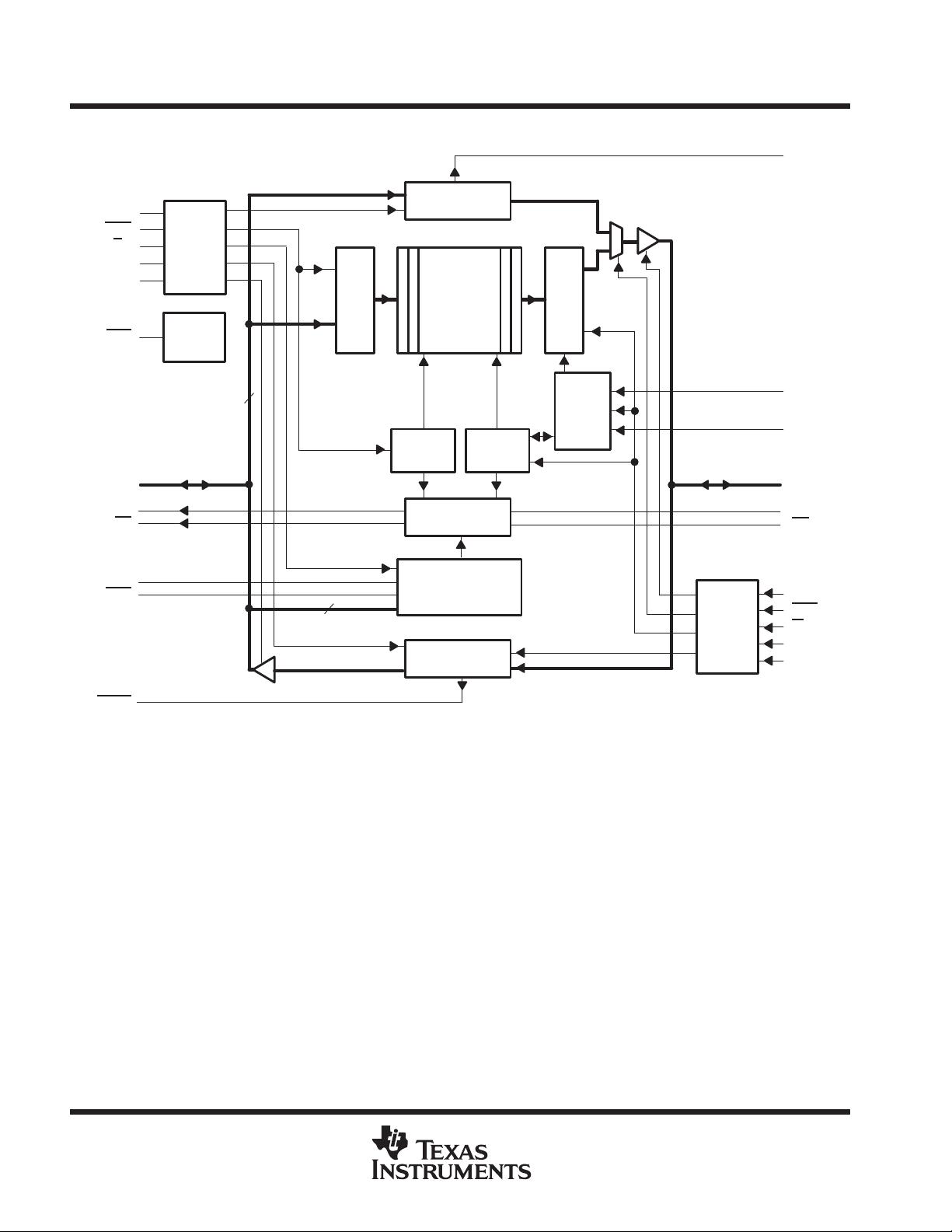
The 512 × 36, 1024 × 36, and 2048 × 36 dual-port SRAM FIFOs buffer data from port A to port B. The FIFO
memories have retransmit capability, which allows previously read data to be accessed again. The FIFOs have
flags to indicate empty and full conditions and two programmable flags (almost full and almost empty) to indicate
when a selected number of words is stored in memory. Communication between each port takes place with two
36-bit mailbox registers. Each mailbox register has a flag that signals when new mail has been stored. Two or
more devices are used in parallel to create wider data paths. Expansion also is possible in word depth.
The SN74ALVC3631/41/51 are synchronous FIFOs, which means each port employs a synchronous interface.
All data transfers through a port are gated to the low-to-high transition of a continuous (free-running) port clock
by enable signals. The continuous clocks for each port are independent of one another and can be
asynchronous or coincident. The enables for each port are arranged to provide a simple interface between
microprocessors and/or buses with synchronous control.
The input-ready (IR) flag and almost-full (AF
) flag of the FIFOs are two-stage, synchronized to CLKA. The
output-ready (OR) flag and almost-empty (AE) flag of the FIFOs are two-stage, synchronized to CLKB. Offset
values for AF and AE are programmed from port A or through a serial input.
The SN74ALVC3631/41/51 are characterized for operation from 0°C to 70°C.
For more information on this device family, see the following application reports:
D
FIFO Patented Synchronous Retransmit: Programmable DSP-Interface Application for FIR Filtering
(literature number SCAA009)
D
FIFO Mailbox-Bypass Registers: Using Bypass Registers to Initialize DMA Control
(literature number SCAA007)
D
Metastability Performance of Clocked FIFOs
(literature number SCZA004)
D
FIFO Architecture, Functions, and Applications
(literature number SCAA042)
D
Optimizing DSP-Based Digital Filters With Application-Specific FIFOs
(literature number SCAA021)
D
FIFO Memories: Surface-Mount Packages for PCMCIA Applications
(literature number SDMA001A)
D
Interfacing TI Clocked FIFOs with TI Floating-Point DSPs
(literature number SCAA005A)
Copyright 2000, Texas Instruments Incorporated
PRODUCTION DATA information is current as of publication date.
Products conform to specifications per the terms of Texas Instruments
standard warranty. Production processing does not necessarily include
testing of all parameters.
Please be aware that an important notice concerning availability, standard warranty, and use in critical applications of
Texas Instruments semiconductor products and disclaimers thereto appears at the end of this data sheet.


 我的内容管理
展开
 我的资源
快来上传第一个资源
 我的收益 登录查看自己的收益
 我的积分
登录查看自己的积分
 我的C币
登录后查看C币余额
 我的收藏
我的收藏  我的下载
我的下载  下载帮助
下载帮助 
 前往需求广场,查看用户热搜

 信息提交成功