
SN74ALS236
64 × 4
ASYNCHRONOUS FIRST-IN, FIRST-OUT MEMORY
SDAS107C – OCTOBER 1986 – REVISED APRIL 1998
1
POST OFFICE BOX 655303 • DALLAS, TEXAS 75265
D
Asynchronous Operation
D
Organized as 64 Words by 4 Bits
D
Data Rates up to 30 MHz
D
3-State Outputs
D
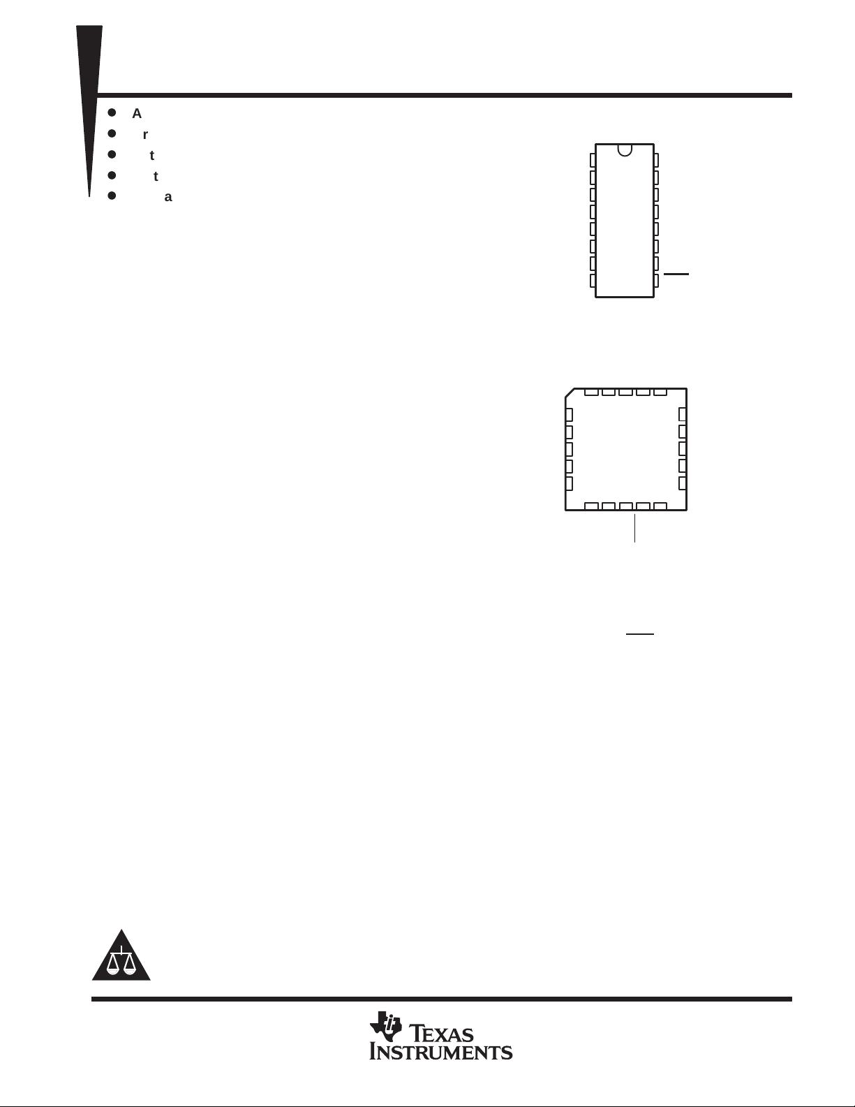
Package Options Include Plastic
Small-Outline Package (DW), Plastic
J-Leaded Chip Carriers (FN), and Standard
Plastic 300-mil DIPs (N)
description
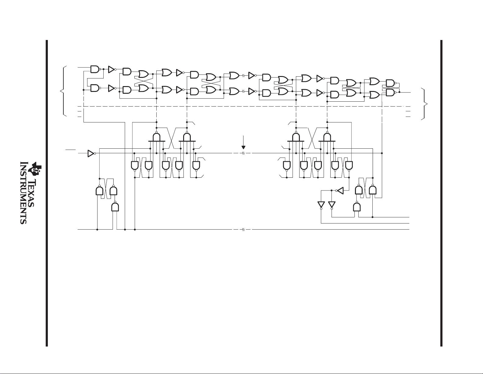
The SN74ALS236 is a 256-bit memory utilizing
advanced low-power Schottky IMPACT
technology. It features high speed with fast
fall-through times and is organized as 64 words by
4 bits.
A first-in, first-out (FIFO) memory is a storage
device that allows data to be written into and read
from its array at independent data rates. The
SN74ALS236 is designed to process data at rates
up to 30 MHz in a bit-parallel format, word by
word.
Data is written into memory on the rising edge of
the shift-in (SI) input. When SI goes low, the first
data word ripples through to the output (see
Figure 1). As the FIFO fills up, the data words
stack up in the order they were written. When the
FIFO is full, additional shift-in pulses have no
effect. Data is shifted out of memory on the falling
edge of the shift-out (SO) input (see Figure 2). When the FIFO is empty, additional SO pulses have no effect.
The last data word remains at the outputs until a new word falls through or reset (RST
) goes low.
Status of the SN74ALS236 FIFO memory is monitored by the output-ready (OR) and input-ready (IR) flags.
When OR is high, valid data is available at the outputs. OR is low when SO is high and stays low when the FIFO
is empty. IR is high when the inputs are ready to receive more data. IR is low when SI is high and stays low when
the FIFO is full.
When the FIFO is empty, input data is shifted to the output automatically when SI goes low. If SO is held high
during this time, the OR flag pulses high, indicating valid data at the outputs (see Figure 3).
When the FIFO is full, data is shifted in automatically by holding SI high and taking SO low. One propagation
delay after SO goes low, IR goes high. If SI is still high when IR goes high, data at the inputs is automatically
shifted in. Since IR is normally low when the FIFO is full and SI is high, only a high-level pulse is seen on the
IR output (see Figure 4).
Copyright 1998, Texas Instruments Incorporated
PRODUCTION DATA information is current as of publication date.
Products conform to specifications per the terms of Texas Instruments
standard warranty. Production processing does not necessarily include
testing of all parameters.
IMPACT is a trademark of Texas Instruments Incorporated.
NC
IR
SI
D0
D1
D2
D3
GND
DW OR N PACKAGE
(TOP VIEW)
3 2 1 20 19
910111213
4
5
6
7
8
18
17
16
15
14
OR
Q0
NC
Q1
Q2
SI
D0
NC
D1
D2
FN PACKAGE
(TOP VIEW)
NC
NC
RST
Q3
SO
D3
GND
NC
V
CC
IR
1
2
3
4
5
6
7
8
16
15
14
13
12
11
10
9
V
CC
SO
OR
Q0
Q1
Q2
Q3
RST
NC – No internal connection
Please be aware that an important notice concerning availability, standard warranty, and use in critical applications of
Texas Instruments semiconductor products and disclaimers thereto appears at the end of this data sheet.

剩余10页未读,继续阅读
资源评论


不觉明了
- 粉丝: 7135
- 资源: 5764


最新资源
- 魔术公式轮胎建模的MATLAB GUI.zip
- 曲面边界的格子玻尔兹曼方法的MATLAB实现.zip
- 谱狮子SPM是一个MATLAB代码,它使用谱数值方法求解所谓的锂离子电池单粒子模型SPM.zip
- 脑机接口BCI的MATLAB工具箱.zip
- 三车道交通流元胞自动机matlab实现.zip
- 上海交通大学MTALAB代码中数据融合过程的求解.zip
- 全景图像拼接的MATLAB代码.zip
- 深度高斯过程的matlab.zip
- 机械臂GUI工具箱基于matlab robotics toolbox.zip
- 基本遗传算法MATLAB程序.zip
- 基本光度立体算法的MATLAB实现.zip
- Unity 导出terrian Nav信息供服务使用,或者自己开发需要
- 基于cnn的机翼损失人脸地标定位的Matlab实现.zip
- 基于MATLAB R2016a的二维和三维环境下无人机路径规划问题.zip
- 基于gpuArray的轻量级MATLAB深度学习工具箱.zip
- 基于delaunay的非结构化网格生成器JIGSAW的MATLAB绑定.zip
资源上传下载、课程学习等过程中有任何疑问或建议,欢迎提出宝贵意见哦~我们会及时处理!
点击此处反馈


