没有合适的资源?快使用搜索试试~ 我知道了~
资源推荐
资源详情
资源评论

SN54ACT3632
512 × 36 × 2
CLOCKED BIDIRECTIONAL FIRST-IN, FIRST-OUT MEMORY
SGBS310A – SEPTEMBER 1996 – REVISED APRIL 1998
1
POST OFFICE BOX 655303 • DALLAS, TEXAS 75265
D
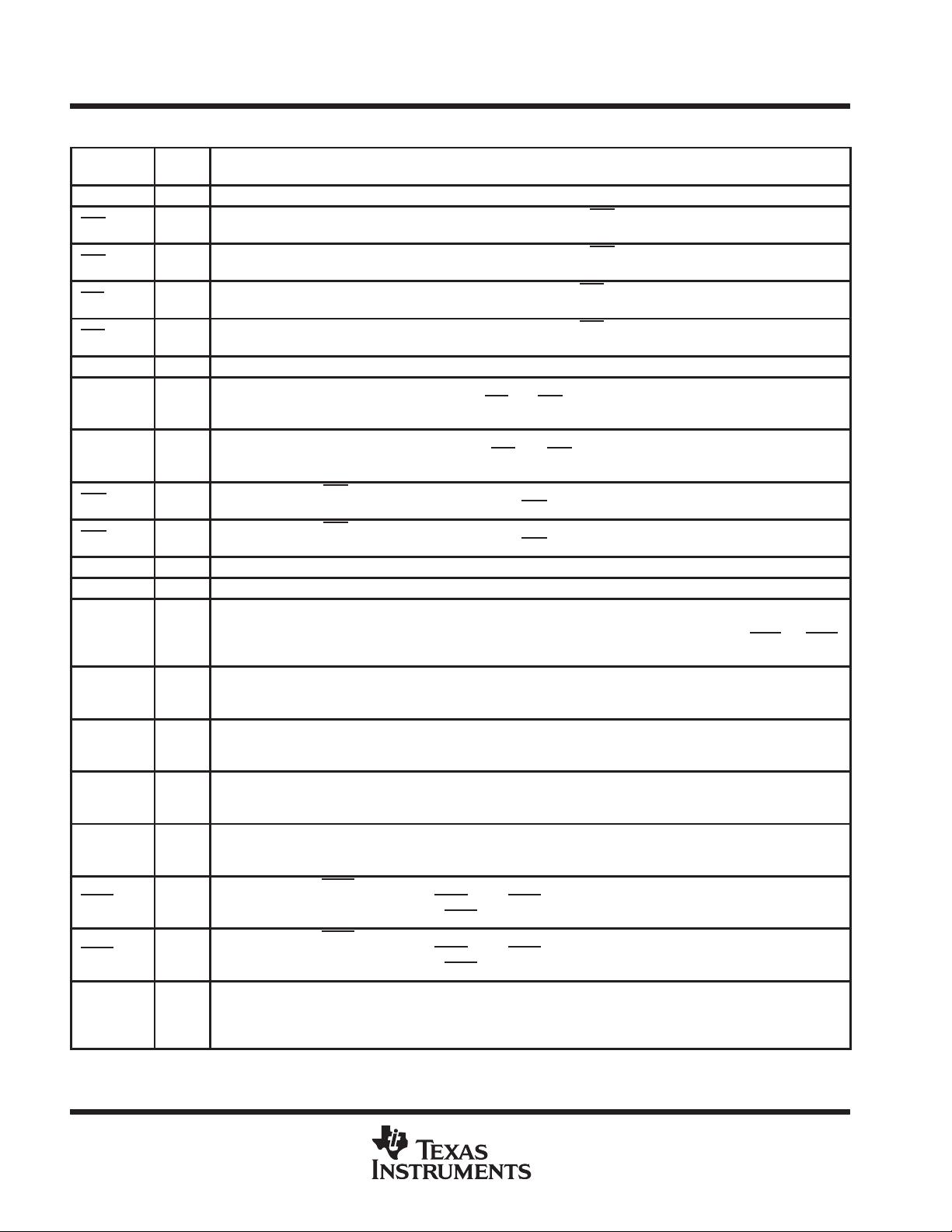
Free-Running CLKA and CLKB Can Be
Asynchronous or Coincident
D
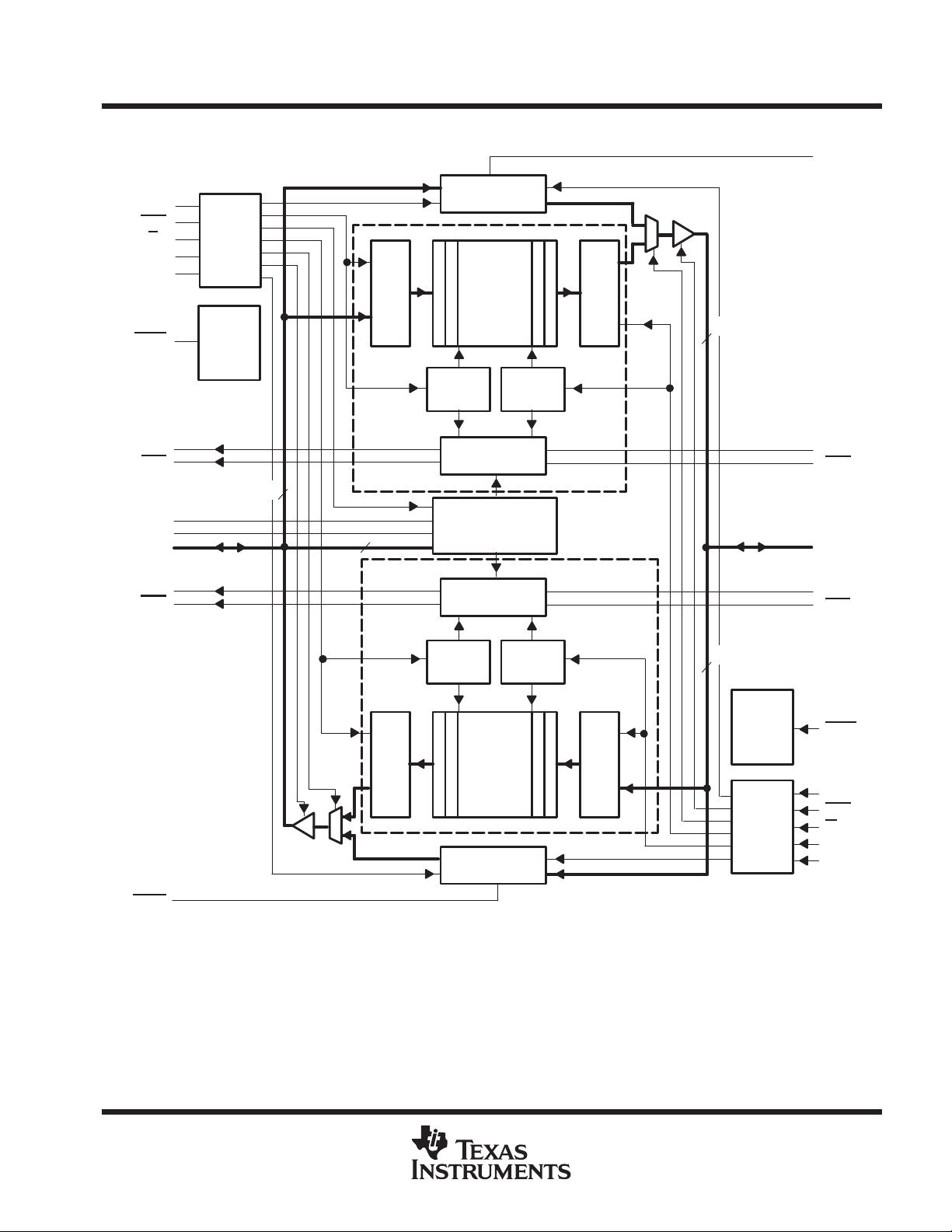
Two Independent 512 × 36 Clocked FIFOs
Buffering Data in Opposite Directions
D
Mailbox-Bypass Register for Each FIFO
D
Programmable Almost-Full and
Almost-Empty Flags
D
Microprocessor Interface Control Logic
D
IRA, ORA, AEA, and AFA Flags
Synchronized by CLKA
D
Released as DESC SMD (Standard
Microcircuit Drawing) 5962-9562801QYA
D
IRB, ORB, AEB, and AFB Flags
Synchronized by CLKB
D
Low-Power 0.8-µm Advanced CMOS
Technology
D
Supports Clock Frequencies up to 50 MHz
D
Fast Access Times of 13 ns
D
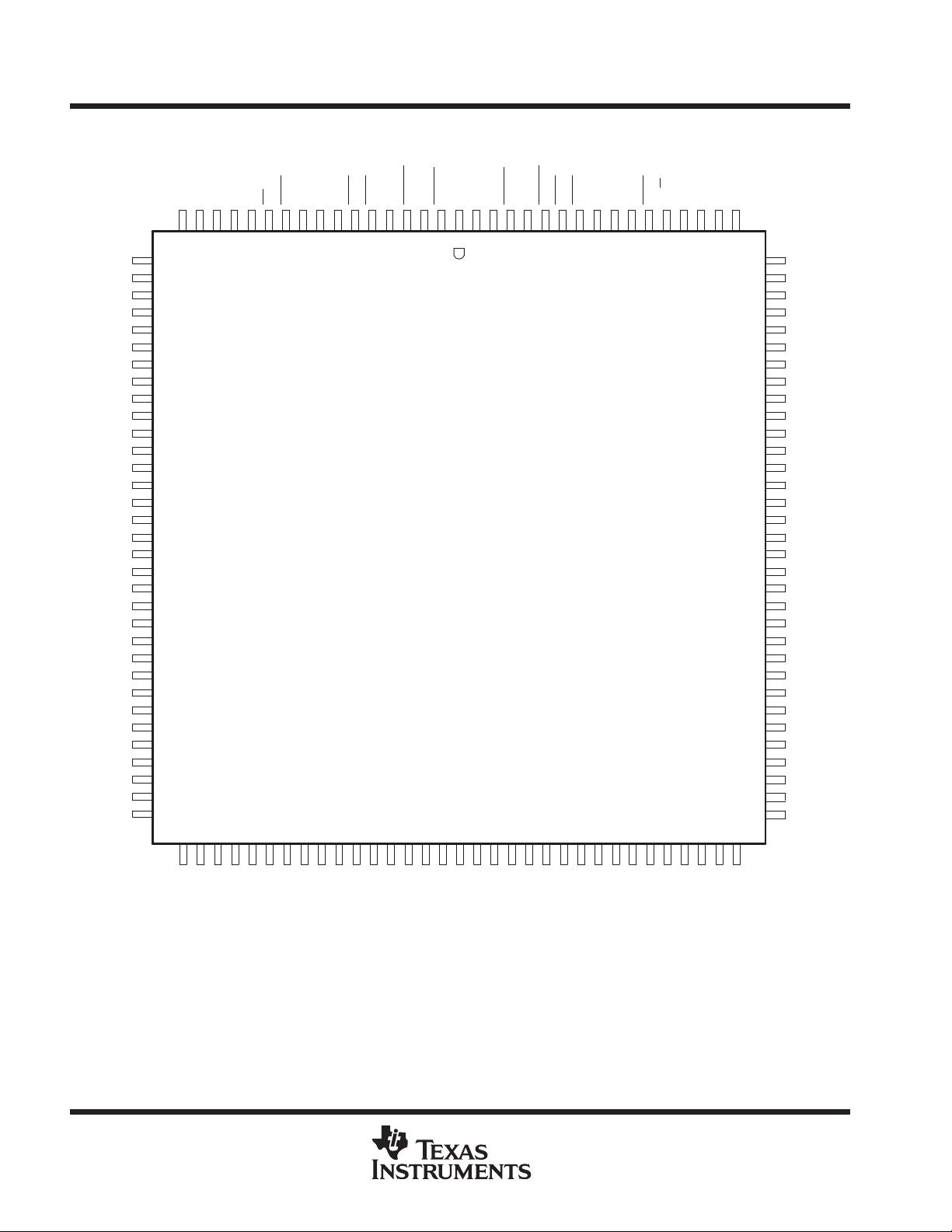
Packaged in 132-Pin Ceramic Quad Flat
Package
description
The SN54ACT3632 is a high-speed, low-power CMOS clocked bidirectional FIFO memory. It supports clock
frequencies up to 50 MHz and has read access times as fast as 11 ns. Two independent 512 × 36 dual-port
SRAM FIFOs on the chip buffer data in opposite directions. Each FIFO has flags to indicate empty and full
conditions and two programmable flags (almost full and almost empty) to indicate when a selected number of
words is stored in memory. Communication between each port can bypass the FIFOs via two 36-bit mailbox
registers. Each mailbox register has a flag to signal when new mail has been stored. Two or more devices can
be used in parallel to create wider data paths.
The SN54ACT3632 is a clocked FIFO, which means each port employs a synchronous interface. All data
transfers through a port are gated to the low-to-high transition of a port clock by enable signals. The clocks for
each port are independent of one another and can be asynchronous or coincident. The enables for each port
are arranged to provide a simple bidirectional interface between microprocessors and/or buses with
synchronous control.
The input-ready (IRA, IRB) flag and almost-full (AFA
, AFB) flag of a FIFO are two-stage synchronized to the
port clock that writes data to its array. The output-ready (ORA, ORB) flag and almost-empty (AEA
, AEB) flag
of a FIFO are two-stage synchronized to the port clock that reads data from its array. Offset values for the
almost-full and almost-empty flags of both FIFOs can be programmed from port A.
The SN54ACT3632 is characterized for operation over the full military temperature range of –55°C to 125°C.
For more information on this device family, see the following application reports:
D
FIFO Mailbox-Bypass Registers: Using Bypass Registers to Initialize DMA Control
(literature number SCAA007)
D
Interfacing TI Clocked FIFOs With TI Floating-Point Digital Signal Processors
(literature number SCAA005)
D
Metastability Performance of Clocked FIFOs
(literature number SCZA004)
Copyright 1998, Texas Instruments Incorporated
PRODUCTION DATA information is current as of publication date.
Products conform to specifications per the terms of Texas Instruments
standard warranty. Production processing does not necessarily include
testing of all parameters.
Please be aware that an important notice concerning availability, standard warranty, and use in critical applications of
Texas Instruments semiconductor products and disclaimers thereto appears at the end of this data sheet.
On products compliant to MIL-PRF-38535, all parameters are tested
unless otherwise noted. On all other products, production
processing does not necessarily include testing of all parameters.

SN54ACT3632
512 × 36 × 2
CLOCKED BIDIRECTIONAL FIRST-IN, FIRST-OUT MEMORY
SGBS310A – SEPTEMBER 1996 – REVISED APRIL 1998
2
POST OFFICE BOX 655303 • DALLAS, TEXAS 75265
NC
B35
B34
B33
B32
GND
B31
B30
B29
B28
B27
B26
V
CC
B25
B24
GND
B23
B22
B21
B20
B19
B18
GND
B17
B16
V
CC
B15
B14
B13
B12
GND
NC
NC
NC
NC
A35
A34
A33
A32
V
CC
A31
A30
GND
A29
A28
A27
A26
A25
A24
A23
GND
A22
V
CC
A21
A20
A19
A18
GND
A17
A16
A15
A14
A13
V
CC
A12
NC
HFP PACKAGE
(TOP VIEW)
NC
NC
V
CLKB
ENB
W/RB
CSB
GND
IRB
ORB
AFB
AEB
MBF1
MBB
RST2
FS1
GND
FS0
RST1
MBA
MBF2
AEA
AFA
ORA
IRA
CSA
W/RA
ENA
CLKA
GND
NC
NC
B11
B10
B9
B8
B7
CC
B6
GND
B5
B4
B3
B2
B1
B0
GND
A0
A1
A2
A3
A4
A5
GND
A6
A7
A8
A9
A10
A11
GND
NC
NC
CC
V
CC
V
CC
V
CC
V
18
19
20
21
22
23
24
25
26
27
28
29
30
31
32
33
34
35
36
37
38
39
40
41
42
43
44
45
46
47
48
49
50
116
115
114
113
112
111
110
109
108
107
106
105
104
103
102
101
100
99
98
97
96
95
94
93
92
91
90
89
88
87
86
85
84
NC – No internal connection
17 16 15 14 13 12 11 10 9 8 7 6 5 4 3 2 1 132 130 128 126 124 122 120 118
131 129 127 125 123 121 119 117
51 52 53 54 55 56 57 58 59 60 61 62 63 64 65 66 67 68 70 72 74 76 78 80 8269 71 73 75 77 79 81 83

SN54ACT3632
512 × 36 × 2
CLOCKED BIDIRECTIONAL FIRST-IN, FIRST-OUT MEMORY
SGBS310A – SEPTEMBER 1996 – REVISED APRIL 1998
3
POST OFFICE BOX 655303 • DALLAS, TEXAS 75265
functional block diagram
Port-A
Control
Logic
CLKA
CSA
W/RA
ENA
MBA
FIFO1,
Mail1
Reset
Logic
RST1
512 × 36
SRAM
Input Register
Output Register
Mail1
Register
Write
Pointer
Read
Pointer
Status-Flag
Logic
Programmable-
Flag
Offset Registers
Status-Flag
Logic
Read
Pointer
Write
Pointer
512 × 36
SRAM
Input Register
Output Register
Mail2
Register
Port-B
Control
Logic
IRA
AFA
FS0
FS1
A0–A35
ORA
AEA
MBF2
FIFO2,
Mail2
Reset
Logic
MBF1
ORB
AEB
B0–B35
IRB
AFB
RST2
CLKB
CSB
W/RB
ENB
MBB
FIFO1
FIFO2
9
36
36
36

SN54ACT3632
512 × 36 × 2
CLOCKED BIDIRECTIONAL FIRST-IN, FIRST-OUT MEMORY
SGBS310A – SEPTEMBER 1996 – REVISED APRIL 1998
4
POST OFFICE BOX 655303 • DALLAS, TEXAS 75265
Terminal Functions
TERMINAL
NAME
I/O DESCRIPTION
A0–A35 I/O Port-A data. The 36-bit bidirectional data port for side A.
AEA
O
(port A)
Port-A almost-empty flag. Programmable flag synchronized to CLKA. AEA is low when the number of words in FIFO2
is less than or equal to the value in the almost-empty A offset register, X2.
AEB
O
(port B)
Port-B almost-empty flag. Programmable flag synchronized to CLKB. AEB is low when the number of words in FIFO1
is less than or equal to the value in the almost-empty B offset register, X1.
AFA
O
(port A)
Port-A almost-full flag. Programmable flag synchronized to CLKA. AFA is low when the number of empty locations
in FIFO1 is less than or equal to the value in the almost-full A offset register, Y1.
AFB
O
(port B)
Port-B almost-full flag. Programmable flag synchronized to CLKB. AFB is low when the number of empty locations
in FIFO2 is less than or equal to the value in the almost-full B offset register, Y2.
B0–B35 I/O Port-B data. The 36-bit bidirectional data port for side B.
CLKA I
Port-A clock. CLKA is a continuous clock that synchronizes all data transfers through port A and can be
asynchronous or coincident to CLKB. IRA, ORA, AFA
, and AEA are all synchronized to the low-to-high transition of
CLKA.
CLKB I
Port-B clock. CLKB is a continuous clock that synchronizes all data transfers through port B and can be
asynchronous or coincident to CLKA. IRB, ORB, AFB
, and AEB are synchronized to the low-to-high transition of
CLKB.
CSA
I
Port-A chip select. CSA must be low to enable a low-to-high transition of CLKA to read or write data on port A. The
A0–A35 outputs are in the high-impedance state when CSA
is high.
CSB
I
Port-B chip select. CSB must be low to enable a low-to-high transition of CLKB to read or write data on port B. The
B0–B35 outputs are in the high-impedance state when CSB
is high.
ENA I Port-A enable. ENA must be high to enable a low-to-high transition of CLKA to read or write data on port A.
ENB I Port-B enable. ENB must be high to enable a low-to-high transition of CLKB to read or write data on port B.
FS1, FS0 I
Flag-offset selects. The low-to-high transition of a FIFO reset input latches the values of FS0 and FS1. If either FS0
or FS1 is high when a reset input goes high, one of three preset values is selected as the offset for the FIFO almost-full
and almost-empty flags. If both FIFOs are reset simultaneously and both FS0 and FS1 are low when RST1
and RST2
go high, the first four writes to FIFO1 program the almost-full and almost-empty offsets for both FIFOs.
IRA
O
(port A)
Input-ready flag. IRA is synchronized to the low-to-high transition of CLKA. When IRA is low, FIFO1 is full and writes
to its array are disabled. IRA is set low when FIFO1 is reset and is set high on the second low-to-high transition of
CLKA after reset.
IRB
O
(port B)
Input-ready flag. IRB is synchronized to the low-to-high transition of CLKB. When IRB is low, FIFO2 is full and writes
to its array are disabled. IRB is set low when FIFO2 is reset and is set high on the second low-to-high transition of
CLKB after reset.
MBA I
Port-A mailbox select. A high level on MBA chooses a mailbox register for a port-A read or write operation. When
the A0–A35 outputs are active, a high level on MBA selects data from the mail2 register for output and a low level
selects FIFO2 output-register data for output.
MBB I
Port-B mailbox select. A high level on MBB chooses a mailbox register for a port-B read or write operation. When
the B0–B35 outputs are active, a high level on MBB selects data from the mail1 register for output and a low level
selects FIFO1 output-register data for output.
MBF1
O
Mail1 register flag. MBF1 is set low by the low-to-high transition of CLKA that writes data to the mail1 register. Writes
to the mail1 register are inhibited while MBF1
is low. MBF1 is set high by a low-to-high transition of CLKB when a
port-B read is selected and MBB is high. MBF1
is set high when FIFO1 is reset.
MBF2
O
Mail2 register flag. MBF2 is set low by the low-to-high transition of CLKB that writes data to the mail2 register. Writes
to the mail2 register are inhibited while MBF2
is low. MBF2 is set high by a low-to-high transition of CLKA when a
port-A read is selected and MBA is high. MBF2
also is set high when FIFO2 is reset.
ORA
O
(port A)
Output-ready flag. ORA is synchronized to the low-to-high transition of CLKA. When ORA is low, FIFO2 is empty
and reads from its memory are disabled. Ready data is present on the output register of FIFO2 when ORA is high.
ORA is forced low when FIFO2 is reset and goes high on the third low-to-high transition of CLKA after a word is loaded
to empty memory.

SN54ACT3632
512 × 36 × 2
CLOCKED BIDIRECTIONAL FIRST-IN, FIRST-OUT MEMORY
SGBS310A – SEPTEMBER 1996 – REVISED APRIL 1998
5
POST OFFICE BOX 655303 • DALLAS, TEXAS 75265
Terminal Functions (Continued)
TERMINAL
NAME
I/O DESCRIPTION
ORB
O
(port B)
Output-ready flag. ORB is synchronized to the low-to-high transition of CLKB. When ORB is low, FIFO1 is empty
and reads from its memory are disabled. Ready data is present on the output register of FIFO1 when ORB is high.
ORB is forced low when FIFO1 is reset and goes high on the third low-to-high transition of CLKB after a word is loaded
to empty memory.
RST1
I
FIFO1 reset. To reset FIFO1, four low-to-high transitions of CLKA and four low-to-high transitions of CLKB must
occur while RST1
is low. The low-to-high transition of RST1 latches the status of FS0 and FS1 for AFA and AEB offset
selection. FIFO1 must be reset upon power up before data is written to its RAM.
RST2
I
FIFO2 reset. To reset FIFO2, four low-to-high transitions of CLKA and four low-to-high transitions of CLKB must
occur while RST2
is low. The low-to-high transition of RST2 latches the status of FS0 and FS1 for AFB and AEA offset
selection. FIFO2 must be reset upon power up before data is written to its RAM.
W/RA
I
Port-A write/read select. A high on W/RA selects a write operation and a low selects a read operation on port A for
a low-to-high transition of CLKA. The A0–A35 outputs are in the high-impedance state when W/R
A is high.
W/RB
I
Port-B write/read select. A low on W/RB selects a write operation and a high selects a read operation on port B for
a low-to-high transition of CLKB. The B0–B35 outputs are in the high-impedance state when W
/RB is low.
detailed description
reset
The FIFO memories of the SN54ACT3632 are reset separately by taking their reset (RST1
, RST2) inputs low
for at least four port-A clock (CLKA) and four port-B clock (CLKB) low-to-high transitions. The reset inputs can
switch asynchronously to the clocks. A FIFO reset initializes the internal read and write pointers and forces the
input-ready flag (IRA, IRB) low, the output-ready flag (ORA, ORB) low, the almost-empty flag (AEA
, AEB) low,
and the almost-full flag (AFA
, AFB) high. Resetting a FIFO also forces the mailbox flag (MBF1, MBF2) of the
parallel mailbox register high. After a FIFO is reset, its input-ready flag is set high after two clock cycles to begin
normal operation. A FIFO must be reset after power up before data is written to its memory.
A low-to-high transition on a FIFO reset (RST1
, RST2) input latches the value of the flag-select (FS0, FS1)
inputs for choosing the almost-full and almost-empty offset programming method.
almost-empty flag and almost-full flag offset programming
Four registers in the SN54ACT3632 are used to hold the offset values for the almost-empty and almost-full flags.
The port-B almost-empty flag (AEB
) offset register is labeled X1 and the port-A almost-empty flag (AEA) offset
register is labeled X2. The port-A almost-full flag (AFA
) offset register is labeled Y1 and the port-B almost-full
flag (AFB
) offset register is labeled Y2. The index of each register name corresponds to its FIFO number. The
offset registers can be loaded with preset values during the reset of a FIFO or they can be programmed from
port A (see Table 1).
Table 1. Flag Programming
FS1 FS0 RST1 RST2 X1 AND Y1 REGISTERS
†
X2 AND Y2 REGISTERS
‡
H H ↑ X 64 X
H H X ↑ X 64
H L ↑ X 16 X
H L X ↑ X 16
L H ↑ X 8 X
L H X ↑ X 8
L L ↑ ↑ Programmed from port A Programmed from port A
†
X1 register holds the offset for AEB; Y1 register holds the offset for AFA.
‡
X2 register holds the offset for AEA
; Y2 register holds the offset for AFB.
剩余26页未读,继续阅读
资源评论


不觉明了
- 粉丝: 1604
- 资源: 4372
上传资源 快速赚钱
我的内容管理 展开
我的资源 快来上传第一个资源
我的收益
登录查看自己的收益我的积分 登录查看自己的积分
我的C币 登录后查看C币余额
我的收藏
我的下载
下载帮助


安全验证
文档复制为VIP权益,开通VIP直接复制
