没有合适的资源?快使用搜索试试~ 我知道了~
TI1-SN74ACT72211L.pdf
需积分: 9 0 下载量 131 浏览量
2022-12-11
13:59:14
上传
评论 5
收藏 328KB PDF 举报
温馨提示
试读
21页
TI1-SN74ACT72211L.pdf
资源推荐
资源详情
资源评论
× × × ×
SCAS222 − FEBRUARY 1993 − REVISED JUNE 1993
1
POST OFFICE BOX 655303 • DALLAS, TEXAS 75265
POST OFFICE BOX 1443
• HOUSTON, TEXAS 77251−1443
D Read and Write Clocks Can Be
Asynchronous or Coincident
D Organization:
− SN74ACT72211L − 512 × 9
− SN74ACT72221L − 1024 × 9
− SN74ACT72231L − 2048 × 9
− SN74ACT72241L − 4096 × 9
D Write and Read Cycle Times of 15 ns
D Bit-Width Expandable
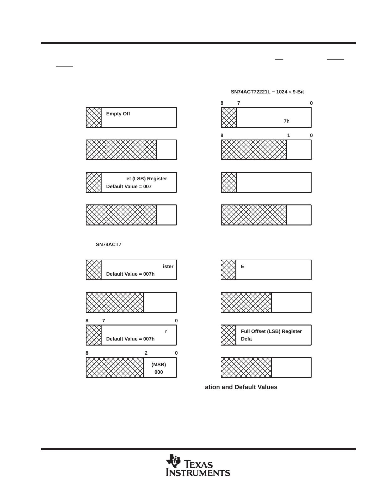
D Empty and Full Flags
D Programmable Almost-Empty and
Almost-Full Flags With Default Offsets
of Empty+7 and Full−7, Respectively
D TTL-Compatible Inputs
D Fully Compatible With the
IDT72211/72221/72231/72241
D Available in 32-Pin Plastic J-Leaded
Chip Carrier (RJ)
description
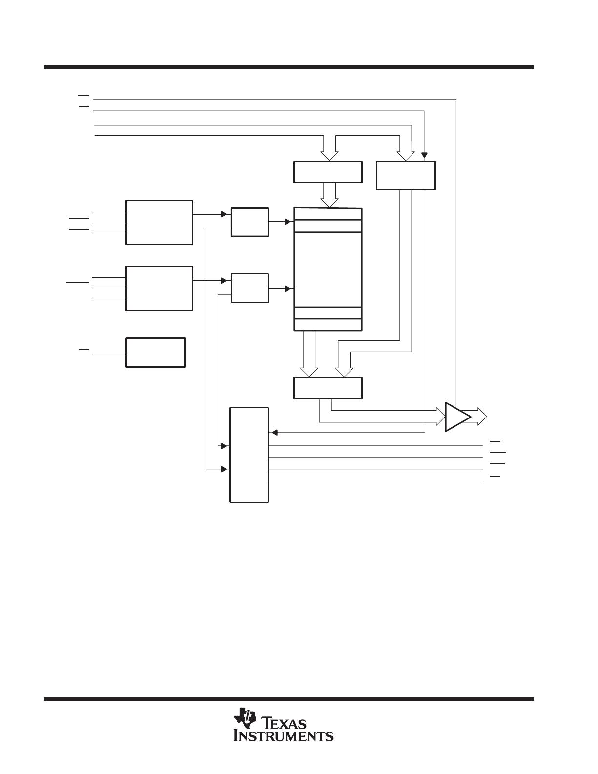
The SN74ACT72211L, SN74ACT72221L, SN74ACT72231L, and SN74ACT72241L are constructed with
CMOS dual-port SRAM and are arranged as 512, 1024, 2048, and 4096 9-bit words, respectively. Internal write
and read address counters provide data throughput on a first-in, first-out (FIFO) basis. Full and empty flags
prevent memory overflow and underflow, and two programmable flags (almost full and almost empty) are
provided.
The SN74ACT72211L, SN74ACT72221L, SN74ACT72231L, and SN74ACT72241L are synchronous FIFOs,
which means the data input port and data output port each employ synchronous control. Write-enable (WEN1
,
WEN2/LD
) signals allow the low-to-high transition of the write clock (WCLK) to store data in memory, and
read-enable (REN1
, REN2) signals allow the low-to-high transition of the read clock (RCLK) to read data from
memory. WCLK and RCLK are independent of one another and can operate asynchronously or be tied together
for single-clock operation.
The empty-flag (EF) output is synchronized to RCLK and the full-flag (FF) output is synchronized to WCLK to
indicate absolute boundary conditions. Write operations are prohibited when FF
is low, and read operations are
prohibited when EF
is low. Two programmable flags, programmable almost empty (PAE) and programmable
almost full (PAF
), can both be programmed to indicate any measure of memory fill. After reset, PAE defaults
to empty+7 and PAF
defaults to full−7. Flag-offset programming control is similar to a memory write with the
use of the load (WEN2/LD
) signal.
These devices are suited for providing a data channel between two buses operating at asynchronous or
synchronous rates. Applications include use as rate buffers for graphics systems and high-speed queues for
communication systems. A 9-bit-wide data path is provided for the transmission of byte data plus a parity bit
or packet-framing information.
The SN74ACT72211L, SN74ACT72221L, SN74ACT72231L, and SN74ACT72241L are characterized for
operation from 0°C to 70°C.
Copyright 1993, Texas Instruments Incorporated
!"#$%&" ' ()##*& %' "! +),-(%&" .%&*/
#".)(&' ("!"#$ &" '+*(!(%&"' +*# &0* &*#$' "! *1%' '&#)$*&'
'&%.%#. 2%##%&3/ #".)(&" +#"(*''4 ."*' "& *(*''%#-3 (-).*
&*'&4 "! %-- +%#%$*&*#'/
3213231
14
5
6
7
8
9
10
11
12
13
29
28
27
26
25
24
23
22
21
RS
WEN1
WCLK
WEN2/LD
V
CC
Q8
Q7
Q6
Q5
D1
D0
PAF
PAE
GND
REN1
RCLK
REN2
OE
430
15 16 17 18 19
EF
FF
Q1
Q3
D2
D3
D4
D5
D6
D7
D8
RJ PACKAGE
(TOP VIEW)
20
Q4
Q0
Q2
Please be aware that an important notice concerning availability, standard warranty, and use in critical applications of
Texas Instruments semiconductor products and disclaimers thereto appears at the end of this data sheet.
× × × ×
SCAS222 − FEBRUARY 1993 − REVISED JUNE 1993
2
POST OFFICE BOX 655303 • DALLAS, TEXAS 75265
POST OFFICE BOX 1443
• HOUSTON, TEXAS 77251−1443
functional block diagram
Input Register
Dual-Port
SRAM
512 × 9 or
1024 × 9 or
2048 × 9 or
4096 × 9
OE
D0−D8
WEN2
RS
LD
Synchronous
Read
Control
Synchronous
Write
Control
Reset
Logic
Status-
Flag
Logic
Read
Pointer
Write
Pointer
Output Register
Offset
Registers
WCLK
REN2
REN1
RCLK
Q0−Q8
EF
PAE
PAF
FF
WEN1
†
†
512 × 9 for the SN74ACT72211L; 1024 × 9 for the SN74ACT72221L; 2048 × 9 for the SN74ACT72231L; 4096 × 9 for the SN74ACT72241L
× × × ×
SCAS222 − FEBRUARY 1993 − REVISED JUNE 1993
3
POST OFFICE BOX 655303 • DALLAS, TEXAS 75265
POST OFFICE BOX 1443
• HOUSTON, TEXAS 77251−1443
Terminal Functions
TERMINAL
I/O
DESCRIPTION
NAME NO.
I/O
DESCRIPTION
D0−D8
6−1,
32−30
I Data inputs
EF 14 O
Empty-flag. When memory is empty, EF is low and further data reads are ignored by the device. When EF is
high, the memory is not empty and data reads are allowed. EF
is synchronized to RCLK by one flip-flop.
FF 15 O
Full-flag. When memory is full, FF is low and data writes are inhibited. FF is synchronized to WCLK by one
flip-flop.
GND 9 Ground
OE 13 I Output-enable. Q0−Q8 are in the high-impedance state when OE is high. Q0−Q8 are active when OE is low.
PAE 8 O
Programmable almost-empty-flag. PAE is low when the FIFO is almost empty based on the value in its offset
register. The default value for the register is empty+7. PAE
is synchronized to RCLK by one flip-flop.
PAF 7 O
Programmable almost-full-flag. PAF is low when the FIFO is almost full based on the value in its offset register.
The default value for the register is full −7. PAF
is synchronized to WCLK by one flip-flop.
Q0−Q8 16−24 O Data outputs
RCLK 11 I
Read-clock. A data read is performed by the low-to-high transition of RCLK when REN1 and REN2 are
asserted and EF
is high.
REN1,
REN2
10,
11
I
Read-enable. Data is read from the FIFO on a low-to-high transition of RCLK when REN1 and REN2 are low
and EF
is high.
RS 29 I
Reset. When RS is set low, the read and write pointers are initialized to the first RAM location and the FIFO
is empty. FF
and PAF are set high, and EF and PAE are set low. Each bit in the data output register is set low
by a device reset. The FIFO must be reset after power up before data is written.
V
CC
Supply voltage
WCLK 27 I
Write-clock. Data is written by the low-to-high transition of WCLK when WEN1 and WEN2/LD are asserted and
FF
is high.
WEN1 28 I
Write-enable 1. WEN1 is the only write enable terminal if the device is configured to have programmable flags.
Data is written on a low-to-high transition of WCLK when WEN1
is low and FF is high. If the FIFO is not
configured for programmable flags, data is written on a low-to-high transition of WCLK when WEN1
and WEN2
are asserted and FF
is high.
WEN2/LD 26 I
Write-enable 2 /load. This is a dual-purpose input. The FIFO can have either two write enables or
programmable flags. To use WEN2/LD
as a WEN2, WEN2/LD must be held high at reset. When WEN2 and
WEN1
are asserted and FF is high, a low-to-high transition of WCLK writes data. To use WEN2/LD as the LD
terminal, it must be held low at reset. In this case, LD is asserted low to write or read the programmable offset
registers.
× × × ×
SCAS222 − FEBRUARY 1993 − REVISED JUNE 1993
4
POST OFFICE BOX 655303 • DALLAS, TEXAS 75265
POST OFFICE BOX 1443
• HOUSTON, TEXAS 77251−1443
detailed description
device reset
A reset is performed by taking the reset (RS
) input low. This initializes both the write and read pointers to the
first memory location. After a reset, the full flag (FF
) and programmable almost-full flag (PAF) are high and the
empty flag (EF
) and programmable almost-empty flag (PAE) are low. Each bit in the data output register
(Q0−Q8) is set low, and the flag offset registers are loaded with the default offset values. A FIFO must be reset
after power up before a write cycle is allowed.
The logic level on the dual-purpose input write enable 2/load (WEN2/LD
) during reset determines its function.
If WEN2/LD
is high when RS returns high at the end of the reset cycle, the input is a second write enable (see
FIFO writes and reads) and the programmable flags (PAF
, PAE) can only use the default values. If WEN2/LD
is low when RS returns high at the end of the reset cycle, the input is the load (LD) enable for writing and reading
flag offset registers (see flag programming).
FIFO writes and reads
Data is written to memory by a low-to-high transition of write clock (WCLK) when write enable 1 (WEN1
) is low,
WEN2/LD
is high, and FF is high. This stores D0−D8 data in the dual-port SRAM and increments the write
pointer.
If no reads are performed after reset (RS
= V
IL
), FF is set low upon the completion of 512 writes to the
SN74ACT72211, 1024 writes to the SN74ACT72221, 2048 writes to the SN74ACT72231, and 4096 writes to
the SN74ACT72241. Attempted write cycles are ignored when FF
is low. FF is set high by the first low-to-high
transition of WCLK after data is read from a full FIFO. FF
and PAF are each synchronized to the low-to-high
transition of WCLK by one flip-flop.
If a device is configured to have two write enables (see device reset), data is read by the low-to-high transition
of read clock (RCLK) when both read enables (REN1
, REN2) are low and EF is high. WEN2/LD must also be
high if the device is configured to have programmable flags. A read from the FIFO puts RAM data on Q0−Q8
and increments the read pointer in the same sequence as the write pointer. New data is not shifted to the output
register while either one or both of the read enables are high.
EF
and PAE are each synchronized to the low-to-high transition of RCLK by one flip-flop. When the device is
empty, the write and read pointers are equal and EF
is set low. Attempted read cycles are ignored while EF is
set low. EF
is set high by the first low-to-high transition of RCLK after data is written to an empty FIFO.
WCLK and RCLK can be asynchronous or coincident to one another. Writing data to FIFO memory is
independent of reading data from FIFO memory and vice versa.
flag programming
When WEN2/LD
is held low during a device reset (RS = V
IL
), the input is the load (LD) enable for flag offset
programming. In this configuration, WEN2/LD
can be used to access the four 8-bit offset registers contained
in the SN74ACT72211L/-72221L/-72231L/-72241L for writing or reading data.
When the device is configured for programmable flags and both WEN2/LD
and WEN1 are low, the first
low-to-high transition of WCLK writes data from the data inputs to the empty offset least significant bit (LSB)
register. The second, third, and fourth low-to-high transitions of WCLK store data in the empty offset most
significant bit (MSB) register, full offset LSB register, and full offset MSB register, respectively, when WEN2/LD
and WEN1 are low. The fifth low-to-high transition of WCLK while WEN2/LD and WEN1 are low writes data to
the empty LSB register again. Figure 1 shows the register sizes and default values for the various device types.
It is not necessary to write to all the offset registers at one time. A subset of the offset registers can be written;
then, by bringing the WEN2/LD input high, the FIFO is returned to normal read and write operation. The next
time WEN2/LD
is brought low, a write operation stores data in the next offset register in sequence.
× × × ×
SCAS222 − FEBRUARY 1993 − REVISED JUNE 1993
5
POST OFFICE BOX 655303 • DALLAS, TEXAS 75265
POST OFFICE BOX 1443
• HOUSTON, TEXAS 77251−1443
flag programming (continued)
The contents of the offset registers can be read to the data outputs when WEN2/LD
is low and both REN1 and
REN2
are low. Low-to-high transitions of RCLK read the register contents to the data outputs. Writes and reads
should not be performed simultaneously on the offset registers (see Figure 1 and Table 1).
ÎÎÎ
ÎÎÎ
ÎÎÎ
Empty Offset (LSB) Register
Default Value = 007h
SN74ACT72211L − 512 × 9-Bit
87 0
810
(MSB)
0
ÎÎÎÎÎÎÎÎÎ
ÎÎÎÎÎÎÎÎÎ
ÎÎÎÎÎÎÎÎÎ
ÎÎÎ
ÎÎÎ
ÎÎÎ
Full Offset (LSB) Register
Default Value = 007h
87 0
810
(MSB)
0
ÎÎÎÎÎÎÎÎÎ
ÎÎÎÎÎÎÎÎÎ
ÎÎÎÎÎÎÎÎÎ
ÎÎÎ
ÎÎÎ
ÎÎÎ
Empty Offset (LSB) Register
Default Value = 007h
SN74ACT72221L − 1024 × 9-Bit
87 0
810
(MSB)
00
ÎÎÎÎÎÎÎÎ
ÎÎÎÎÎÎÎÎ
ÎÎÎÎÎÎÎÎ
ÎÎÎ
ÎÎÎ
ÎÎÎ
Full Offset (LSB) Register
Default Value = 007h
87 0
810
(MSB)
00
ÎÎÎÎÎÎÎÎ
ÎÎÎÎÎÎÎÎ
ÎÎÎÎÎÎÎÎ
ÎÎÎ
ÎÎÎ
ÎÎÎ
ÎÎÎ
Empty Offset (LSB) Register
Default Value = 007h
SN74ACT72231L − 2048 × 9-Bit
87 0
820
(MSB)
000
ÎÎÎÎÎÎÎ
ÎÎÎÎÎÎÎ
ÎÎÎÎÎÎÎ
ÎÎÎ
ÎÎÎ
ÎÎÎ
Full Offset (LSB) Register
Default Value = 007h
87 0
820
(MSB)
000
ÎÎÎÎÎÎÎ
ÎÎÎÎÎÎÎ
ÎÎÎÎÎÎÎ
ÎÎÎ
ÎÎÎ
ÎÎÎ
ÎÎÎ
Empty Offset (LSB) Register
Default Value = 007h
SN74ACT72241L − 4096 × 9-Bit
87 0
830
(MSB)
0000
ÎÎÎÎÎÎÎ
ÎÎÎÎÎÎÎ
ÎÎÎÎÎÎÎ
ÎÎÎ
ÎÎÎ
ÎÎÎ
Full Offset (LSB) Register
Default Value = 007h
87 0
830
(MSB)
0000
ÎÎÎÎÎÎÎ
ÎÎÎÎÎÎÎ
ÎÎÎÎÎÎÎ
Figure 1. Offset Register Location and Default Values
剩余20页未读,继续阅读
资源评论
不觉明了
- 粉丝: 3162
- 资源: 5419
上传资源 快速赚钱
- 我的内容管理 展开
- 我的资源 快来上传第一个资源
- 我的收益 登录查看自己的收益
- 我的积分 登录查看自己的积分
- 我的C币 登录后查看C币余额
- 我的收藏
- 我的下载
- 下载帮助
安全验证
文档复制为VIP权益,开通VIP直接复制
信息提交成功