TI1-TMS416800.pdf

需积分: 0 67 浏览量
更新于2022-12-10
4
收藏 358KB PDF 举报
TI的TMS41x800系列是高性能的16777216位动态随机存取存储器(DRAMs),它们被组织为2097152个8位字。这些器件采用了德州仪器(TI)的尖端增强性能植入式互补金属氧化物半导体(EPIC)技术,旨在实现高速、高可靠性和低功耗。
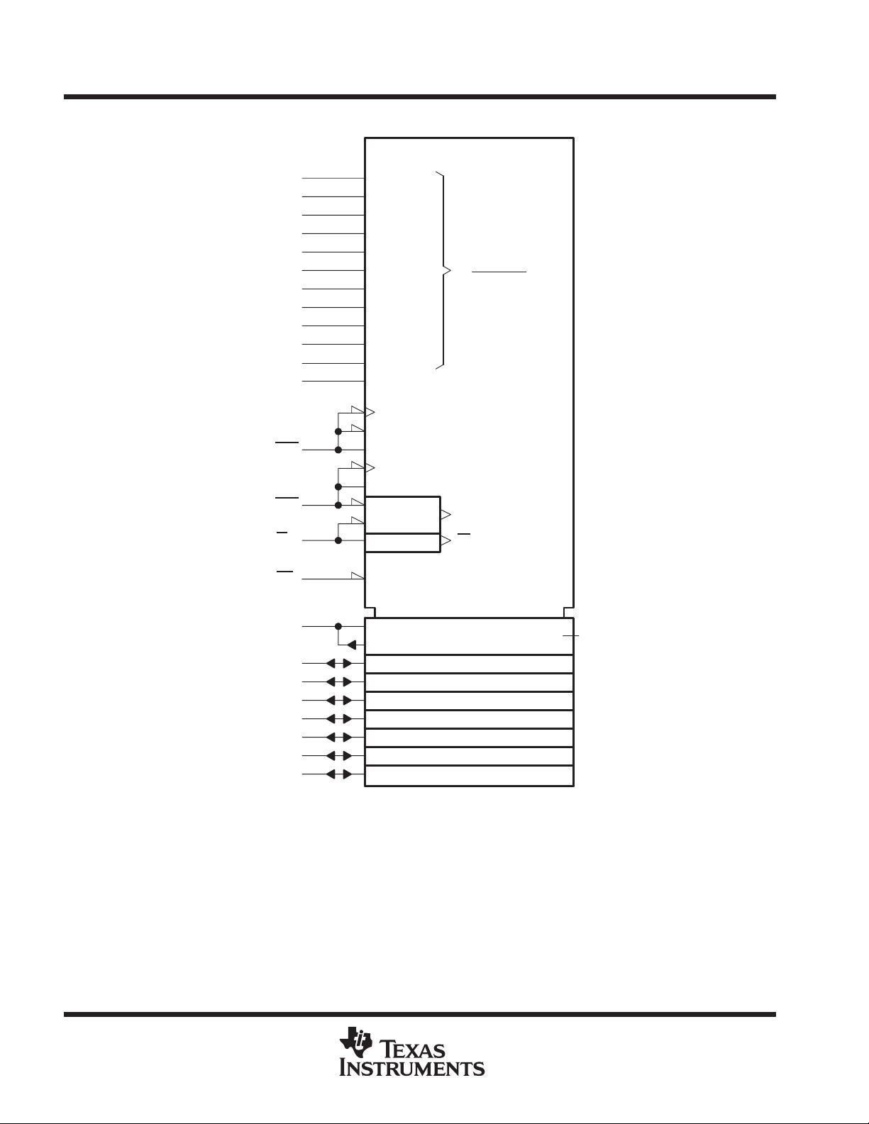
TMS416800和TMS417800是该系列的成员,提供了三种不同的最大RAS访问时间:60ns、70ns和80ns,这使得它们在速度上有多种选择。所有的地址输入和数据输入线都通过片上锁存器进行锁存,简化了系统设计。数据输出则未被锁存,从而增加了系统的灵活性。
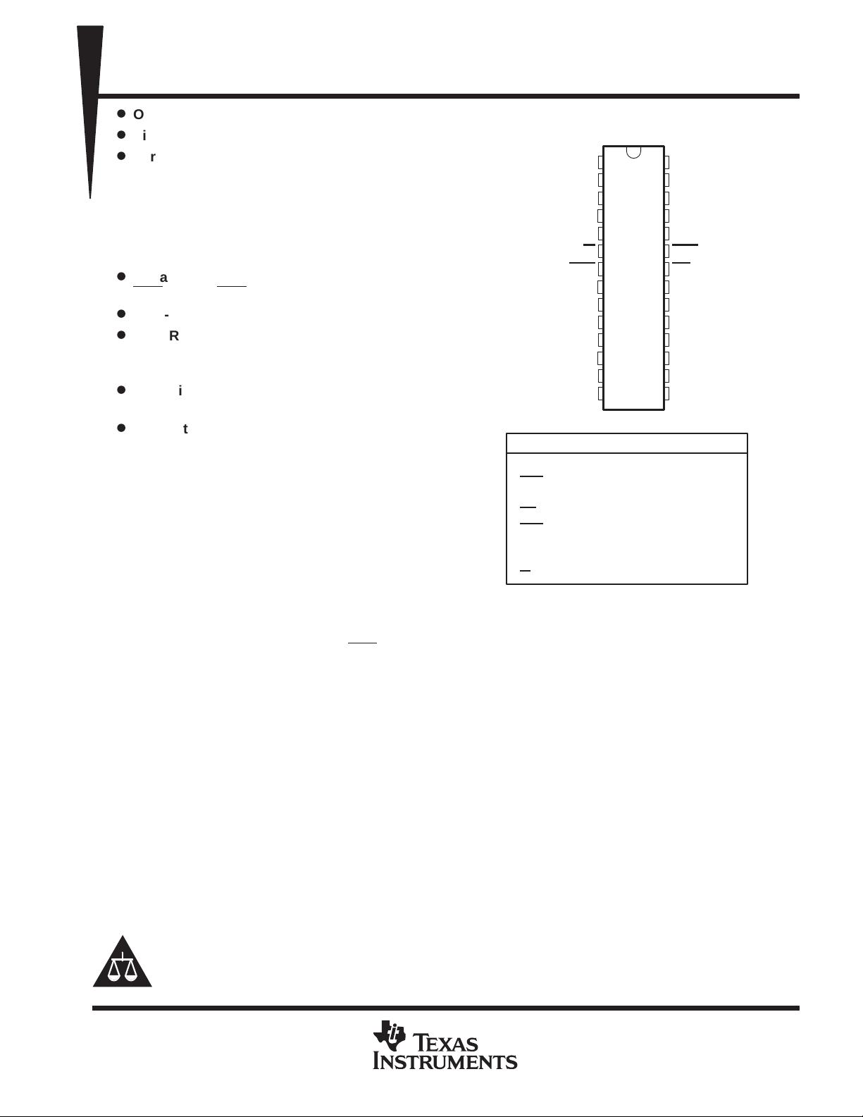
该系列DRAMs采用28引脚塑料表面贴装的小外形J型引脚(SOJ)封装,具有DZ后缀,其工作温度范围为0°C至70°C。值得注意的是,对于TMS417800,A11引脚内部没有连接(NC,无内部连接)。
在功能方面,TMS41x800系列支持增强的页模式操作,包括CAS-Before-RAS(CBR)刷新,这种特性允许更快的数据读取和写入。此外,器件还具有高阻态未锁定输出,这意味着在不需要时,输出可以被设置为高阻抗状态,减少对系统其他部分的影响。
引脚定义如下:
- A0到A11:地址输入,A11在TMS417800中为非连接。
- CAS:列地址选通,用于指定列地址。
- DQ0到DQ7:数据输入/输出引脚,用于传输数据。
- OE:输出使能,控制数据输出的开/关。
- RAS:行地址选通,用于指定行地址。
- VCC:5V电源电压。
- VSS:接地。
- W:写使能,控制数据写入。
封装形式为28引脚的DZ包,适用于表面安装,适合需要紧凑空间的电子设计。
TI在其数据表的末尾提到了关于产品可用性、标准保修以及在关键应用中使用其半导体产品的注意事项和免责声明,用户在使用前应仔细阅读并遵循这些条款。
TMS41x800系列是为高速、高密度存储需求设计的DRAM解决方案,适用于需要快速数据访问和可靠性的各种系统,如计算机、服务器、嵌入式系统和其他电子设备。其优化的EPIC技术确保了低功耗和高可靠性,而灵活的输出设计和多种访问时间选项则满足了不同应用的需求。
TMS416800, TMS417800
2097152-WORD BY 8-BIT HIGH-SPEED DRAMS
SMKS883A – OCTOBER 1995 – REVISED MARCH 1996
1
POST OFFICE BOX 1443 • HOUSTON, TEXAS 77251–1443
D
Organization...2097152 × 8
D
Single 5 V Power Supply (±10% Tolerance)
D
Performance Ranges:
ACCESS ACCESS ACCESS READ OR
TIME TIME TIME WRITE
t
RAC
t
CAC
t
AA
CYCLE
MAX MAX MAX MIN
’41x800-60 60 ns 15 ns 30 ns 110 ns
’41x800-70 70 ns 18 ns 35 ns 130 ns
’41x800-80 80 ns 20 ns 40 ns 150 ns
D
Enhanced Page-Mode Operation With
CAS
-Before-RAS (CBR) Refresh
D
High-Impedance State Unlatched Output
D
High-Reliability Plastic 28-Lead
400-Mil-Wide Surface-Mount Small-Outline
J-Lead (SOJ) Package
D
Operating Free-Air Temperature Range
0°C to 70°C
D
Fabricated Using Enhanced Performance
Implanted CMOS (EPIC
) Technology by
Texas Instruments (TI)
description
The TMS41x800 series is a set of high-speed,
16777216-bit dynamic random-access memo-
ries (DRAMs) organized as 2097152 words of
eight bits each. It employs TI’s state-of-the-art
EPIC technology for high performance, reliability,
and low power.
These devices feature maximum RAS
access
times of 60 ns, 70 ns, and 80 ns. All addresses and
data-in lines are latched on-chip to simplify
system design. Data out is unlatched to allow
greater system flexibility.
The TMS416800 and TMS417800 are offered in
a 28-lead plastic surface-mount SOJ package
(DZ suffix). This package is characterized for
operation from 0°C to 70°C.
Please be aware that an important notice concerning availability, standard warranty, and use in critical applications of
Texas Instruments semiconductor products and disclaimers thereto appears at the end of this data sheet.
PIN NOMENCLATURE
A0–A11
†
Address Inputs
CAS
Column-Address Strobe
DQ0–DQ7 Data In/Data Out
OE
Output Enable
RAS
Row-Address Strobe
V
CC
5 V
V
SS
Ground
W
Write Enable
†
A11 is NC (no internal connection) for TMS417800.
1
2
3
4
5
6
7
8
9
10
11
12
13
14
28
27
26
25
24
23
22
21
20
19
18
17
16
15
V
CC
DQ0
DQ1
DQ2
DQ3
W
RAS
A11
†
A10
A0
A1
A2
A3
V
CC
V
SS
DQ7
DQ6
DQ5
DQ4
CAS
OE
A9
A8
A7
A6
A5
A4
V
SS
DZ PACKAGE
(TOP VIEW)
PRODUCTION DATA information is current as of publication date.
Products conform to specifications per the terms of Texas Instruments
standard warranty. Production processing does not necessarily include
testing of all parameters.
Copyright 1996, Texas Instruments Incorporated
EPIC and TI are trademarks of Texas Instruments Incorporated.


剩余24页未读,继续阅读
2022-12-10 上传
164 浏览量
2022-12-10 上传
2022-12-10 上传
171 浏览量
145 浏览量
120 浏览量
138 浏览量
2022-12-10 上传
2022-12-10 上传
2022-12-10 上传
资源评论


不觉明了
- 粉丝: 8301
- 资源: 5764


最新资源
- 西门子数控系统调试与通讯:828D、840D、808D的参数配置、梯形图修改及外部IO增加案例分享,西门子数控系统调试与配置手册:涉及828D、840D与808D系统的参数调整、梯形图修改与外部通讯实
- 中国各类互联网应用的用户规模数据.zip
- 中国各省地图(包含港澳台) 山西(shanxi)陕西(shanxi1)
- E000620医院体检医疗健康类网站模板+PHP+Mysql+响应式+CMS+建站模板
- 中国各省对应各市级地图json
- 大模型基础-30分钟一文了解大模型基础知识(人工智能必读).zip
- COMSOL模拟:二氧化碳充装与输气管道泄漏的耦合温度场分析,输出速度与温度分布,COMSOL模拟:二氧化碳充装与输气管道泄漏的耦合温度场分析,输出速度与温度分布,comsol 二氧化碳充装二氧化碳输
- 基于python开发的简单的windows桌面画笔功能,全部使用快捷键操作(python源码+图文教程),开箱即用,非常优质的资源
- C#上位机与西门子PLC通讯教程:数据读取存储、报表生成、报警历史查询及变量自定义配置实战案例详解,C#上位机与西门子PLC通讯教程:数据读取存储、报表生成、报警历史查询及变量自定义配置实战案例详解
- 基于遗传算法的锂电池二阶RC模型参数辨识技术研究-附Matlab程序与多种工况充放电数据集(DST、FUDs、US06、BJDST等八种),基于遗传算法的锂电池二阶RC模型参数辨识技术研究-附Ma
- 利用格子玻尔兹曼方法LBM D1Q3模型在Matlab中模拟一维扩散方程的研究,使用格子玻尔兹曼方法LBM D1Q3模拟一维扩散方程的Matlab实现与应用研究,使用格子玻尔兹曼方法LBM D1Q3模
- 流水线电机变频调速系统设计 MATLAB电路建模仿真
- 2022年美国各州基本经济统计数据.zip
- 基于Transformer的Matlab代码:数据回归与多场景预测工具箱,Transformer在数据回归分析中的应用-基于Matlab代码的实战教学,Transformer回归 Matlab代码
- Sigma-Delta ADC Matlab模型集合:包含CTSD调制器、FFT分析、动态静态特性仿真与教程,方便入门学习,Continuous-Time Sigma-Delta ADC Matlab
- 基于Comsol仿真的兰姆波导波在钢板中的传播及裂隙检测分析,Comsol仿真中兰姆波导波在有限尺寸钢板内传播的裂隙检测技术研究,Comsol仿真无损检测时产生的兰姆波 导波在宽度和厚度有限的钢板中传
