没有合适的资源?快使用搜索试试~ 我知道了~
TI1-TMS416169.pdf
需积分: 0 0 下载量 171 浏览量
2022-12-10
23:06:53
上传
评论 4
收藏 392KB PDF 举报
温馨提示
试读
26页
TI1-TMS416169.pdf
资源推荐
资源详情
资源评论
TMS416169, TMS418169
1048576-WORD BY 16-BIT EXTENDED DATA OUT HIGH-SPEED DRAMS
SMKS886C – MAY1995–REVISED MARCH 1996
1
POST OFFICE BOX 1443 • HOUSTON, TEXAS 77251–1443
D
Organization...1048576 Words by 16 Bits
D
Single 5-V Power Supply
D
Performance Ranges:
ACCESS ACCESS ACCESS READ OR
TIME TIME TIME EDO
t
RAC
t
CAC
t
AA
CYCLE
MAX MAX MAX MIN
’41x169/P-60 60 ns 15 ns 30 ns 25 ns
’41x169/P-70 70 ns 18 ns 35 ns 30 ns
’41x169/P-80 80 ns 20 ns 40 ns 35 ns
D
Extended-Data-Out (EDO) Operation
D
xCAS-Before-RAS (xCBR) Refresh
D
RAS-Only Refresh
– 1024-Cycle Refresh in 16 ms
(TMS418169)
– 4096-Cycle Refresh in 64 ms
(TMS416169)
D
3-State Unlatched Output
D
High-Reliability Plastic 42-Lead (DZ
Suffix) 400-Mil-Wide Surface-Mount (SOJ)
Package
D
Operating Free-Air Temperature Range
0°C to 70°C
D
Texas Instruments Enhanced Performance
Implanted CMOS (EPIC
) Process
description
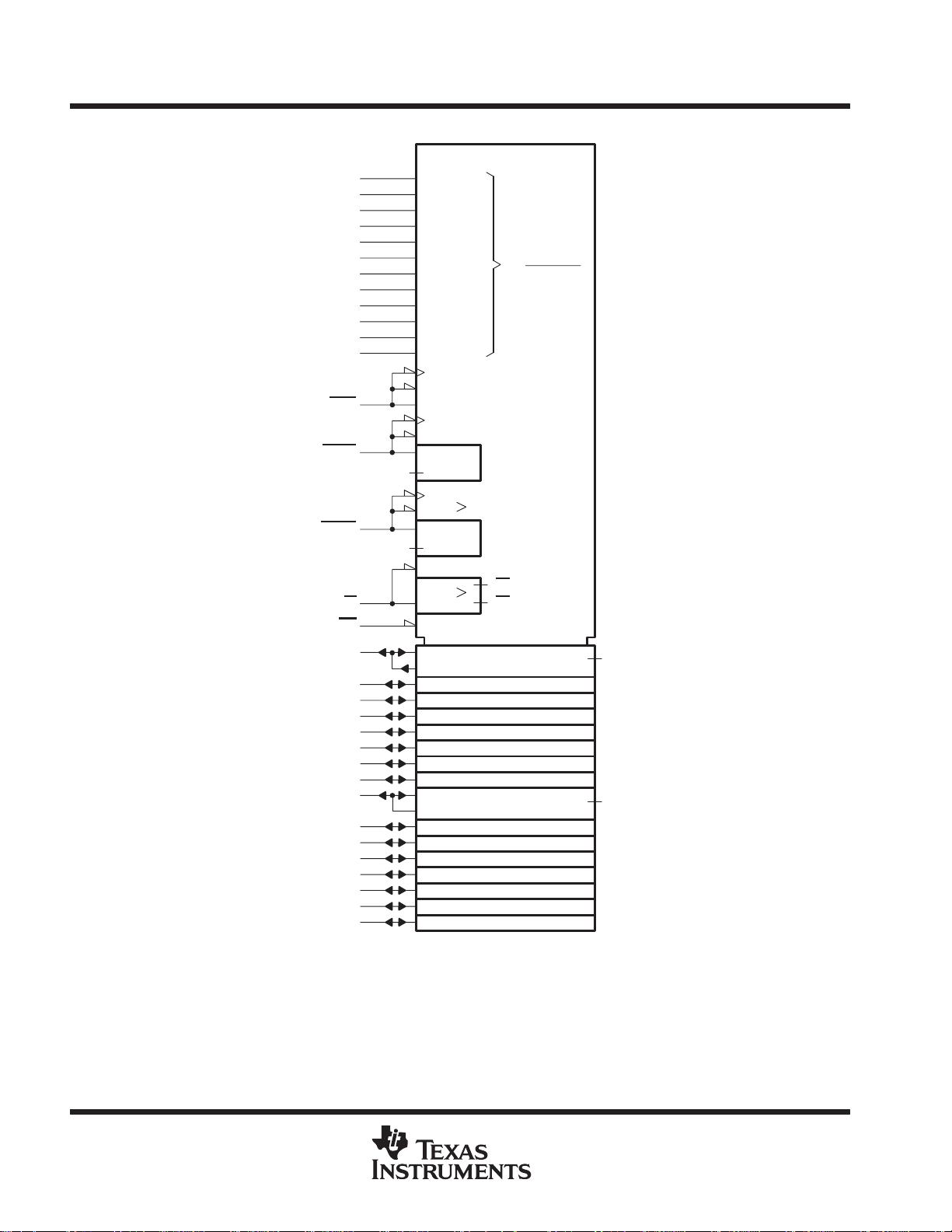
The TMS418169 and the TMS416169 are
high-speed, 16777216-bit dynamic random-ac-
cess memories (DRAMs) organized as 1048576
words of 16 bits each. Both devices employ
state-of-the-art EPIC technology for high perform-
ance, reliability, and low power at low cost.
These devices feature maximum RAS
access
times of 60 ns, 70 ns, and 80 ns. All addresses and
data-in lines are latched on-chip to simplify
system design. Data out is unlatched to allow
greater system flexibility.
The TMS416169 and TMS418169 are offered in a 42-lead plastic surface-mount SOJ (DZ suffix) package. The
package is characterized for operation from 0°C to 70°C.
Please be aware that an important notice concerning availability, standard warranty, and use in critical applications of
Texas Instruments semiconductor products and disclaimers thereto appears at the end of this data sheet.
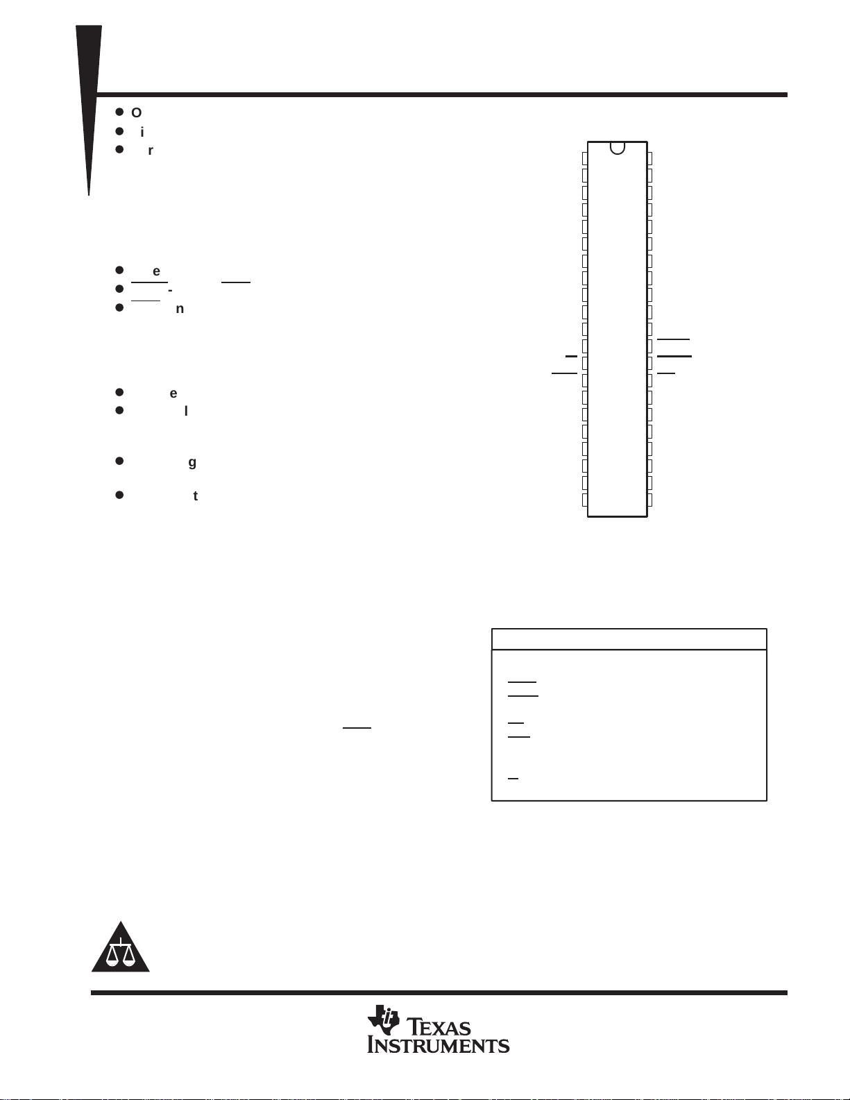
DZ PACKAGE
(TOP VIEW)
PIN NOMENCLATURE
A0–A11 Address Inputs
DQ0– DQ15 Data In/ Data Out
LCAS
Lower Column-Address Strobe
UCAS
Upper Column-Address Strobe
NC No Internal Connection
OE
Output Enable
RAS
Row-Address Strobe
V
CC
5-V Supply
V
SS
Ground
W
Write Enable
1
2
3
4
5
6
7
8
9
10
11
12
13
14
15
16
17
18
19
20
21
42
41
40
39
38
37
36
35
34
33
32
31
30
29
28
27
26
25
24
23
22
V
CC
DQ0
DQ1
DQ2
DQ3
V
CC
DQ4
DQ5
DQ6
DQ7
NC
NC
W
RAS
A11
†
A10
†
A0
A1
A2
A3
V
CC
V
SS
DQ15
DQ14
DQ13
DQ12
V
SS
DQ11
DQ10
DQ9
DQ8
NC
LCAS
UCAS
OE
A9
A8
A7
A6
A5
A4
V
SS
†
A10 and A11 are NC for TMS418169.
EPIC is a trademark of Texas Instruments Incorporated.
PRODUCTION DATA information is current as of publication date.
Products conform to specifications per the terms of Texas Instruments
standard warranty. Production processing does not necessarily include
testing of all parameters.
Copyright 1996, Texas Instruments Incorporated
TMS416169, TMS418169
1048576-WORD BY 16-BIT EXTENDED DATA OUT HIGH-SPEED DRAMS
SMKS886C – MAY1995– REVISED MARCH 1996
2
POST OFFICE BOX 1443 • HOUSTON, TEXAS 77251–1443
logic symbol
†
3
4
5
7
8
9
10
33
34
35
38
39
40
41
36
14
31
30
2
13
29
A0
A1
A2
A3
A4
A5
A6
A7
17
18
19
20
23
24
25
26
DQ1
DQ2
DQ3
DQ4
DQ5
DQ6
DQ7
DQ8
DQ9
DQ10
DQ11
DQ12
DQ13
DQ14
DQ15
DQ0
RAS
LCAS
UCAS
W
RAM 1M × 16
C20[ROW]
G23/[REFRESH ROW]
24[PWR DWN]
C21
G24
&
23C22
A,22D
A8
27
31
C21
G34
&
31
Z31
24,25EN27
34
,25EN37
23C32
23,21D
∇26,27
A, Z26
A,32D
∇36,37
A, Z36
OE
A
0
1 048 575
A9
28
25
20D15/21D7
20D16
20D17
20D8/21D0
A10
‡
16
A11
‡
15
20D18
20D19
†
This symbol is in accordance with ANSI/IEEE Std 91-1984 and IEC Publication 617-12.
The pin numbers shown correspond to the DZ package.
‡
A10 and A11 are NC for TMS418169.
TMS416169, TMS418169
1048576-WORD BY 16-BIT EXTENDED DATA OUT HIGH-SPEED DRAMS
SMKS886C – MAY1995– REVISED MARCH 1996
3
POST OFFICE BOX 1443 • HOUSTON, TEXAS 77251–1443
functional block diagram (TMS416169)
A0
A1
A7
32
16
16
Timing and Control
Column-
Address
Buffers
Row-
Address
Buffers
I/O
Buffers
Data-
In
Reg.
Data-
Out
Reg.
Column Decode
Sense Amplifiers
R
o
w
D
e
c
o
d
e
256K Array
256K Array
256K Array
256K Array
256K Array
256K Array
DQ0–DQ15
RAS UCAS W OE
LCAS
16 of 32
Selection
32
A8–
A11
4
8
12
12
32
32
functional block diagram (TMS418169)
A0
A1
A9
32
16
16
Timing and Control
Column-
Address
Buffers
Row-
Address
Buffers
I/O
Buffers
Data-
In
Reg.
Data-
Out
Reg.
Column Decode
Sense Amplifiers
R
o
w
D
e
c
o
d
e
256K Array
256K Array
256K Array
256K Array
256K Array
256K Array
DQ0–DQ15
RAS
UCAS W OELCAS
16 of 32
Selection
32
10
10
10
32
32
TMS416169, TMS418169
1048576-WORD BY 16-BIT EXTENDED DATA OUT HIGH-SPEED DRAMS
SMKS886C – MAY1995– REVISED MARCH 1996
4
POST OFFICE BOX 1443 • HOUSTON, TEXAS 77251–1443
operation
dual CAS
Two CAS pins (LCAS and UCAS) are provided to give independent control of the 16 data-I/O pins
(DQ0–DQ15), with LCAS
corresponding to DQ0–DQ7 and UCAS corresponding to DQ8–DQ15. For read or
write cycles, the column address is latched on the first xCAS
falling edge. Each xCAS going low enables its
corresponding DQx pin with data associated with the column address latched on the first falling xCAS
edge.
All address setup and hold parameters are referenced to the first falling xCAS
edge.The delay time from xCAS
low to valid data out (see parameter t
CAC
) is measured from each individual xCAS to its corresponding DQx pin.
In order to latch in a new column address, both xCAS
pins must be brought high. The column-precharge time
(see parameter t
CP
) is measured from the last xCAS rising edge to the first xCAS falling edge of the new cycle.
Keeping a column address valid while toggling xCAS
requires a minimum setup time, t
CLCH
. During t
CLCH
, at
least one xCAS
must be brought low before the other xCAS is taken high.
For early-write cycles, the data is latched on the first xCAS
falling edge. Data is written only into the DQs
that have the corresponding xCAS
low. Each xCAS must meet t
CAS
minimum in order to ensure writing into
the storage cell. To latch a new address and new data, all xCAS
pins must be high and meet t
CP
.
extended data out
Extended data out (EDO) allows for data-output rates of up to 40 MHz for 60-ns devices. When keeping the
same row address while selecting random column addresses, the time for row-address setup and hold and
address multiplex is eliminated. The maximum number of columns that can be accessed is determined by the
maximum RAS
low time (t
RASP
).
EDO does not enter the DQs into the high-impedance state with the rising edge of xCAS
. The output remains
valid for the system to latch the data. After xCAS
goes high, the DRAM is decoding the next address. OE and
W
can be used to control the output impedance. Descriptions of OE and W further explain EDO operation
benefit.
address: A0–A11 (TMS416169) and A0–A9 (TMS418169)
Twenty address bits are required to decode one of the 1048576 storage cell locations. For the TMS416169,
12 row-address bits are set up on A0 through A11 and latched onto the chip by RAS
. Eight column-address bits
are set up on A0 through A7 and latched on the chip by the first xCAS
. For the TMS418169, 10 row-address
bits are set up on A0–A9 and latched on the chip by RAS
. Ten column-address bits are set up on A0–A9 and
latched on the chip by the first xCAS
. All addresses must be stable on or before the falling edge of RAS and
xCAS
. RAS is similar to a chip-enable in that it activates the sense amplifiers as well as the row decoder. xCAS
is used as a chip-select, activating its corresponding output buffer and latching the address bits into the
column-address buffers.
write enable (W
)
The read or write mode is selected through W
. A logic high on W selects the read mode and a logic low selects
the write mode. The data input is disabled when the read mode is selected. When W
goes low prior to xCAS
(early write), data out remains in the high-impedance state for the entire cycle, permitting a write operation
independent of the state of OE
. This permits early-write operation to be completed with OE grounded. If W goes
low in an extended-data-out read cycle, the DQs go into the high-impedance state as long as xCAS
is high.
data in (DQ0–DQ15)
Data is written during a write or read-modify-write cycle. Depending on the mode of operation, the falling edge
of xCAS
or W strobes data into the on-chip data latch. In an early-write cycle, W is brought low prior to xCAS
and the data is strobed in by the first occurring xCAS with setup and hold times referenced to this signal. In a
TMS416169, TMS418169
1048576-WORD BY 16-BIT EXTENDED DATA OUT HIGH-SPEED DRAMS
SMKS886C – MAY1995– REVISED MARCH 1996
5
POST OFFICE BOX 1443 • HOUSTON, TEXAS 77251–1443
data in (DQ0–DQ15) (continued)
delayed-write or read-modify-write cycle, xCAS
is already low and the data is strobed in by W with setup and
hold times referenced to this signal. In a delayed-write or read-modify-write cycle, OE
must be high to bring the
output buffers to the high-impedance state prior to impressing data on the I/O lines.
data out (DQ0–DQ15)
Data out is the same polarity as data-in. The output is in the high-impedance (floating) state until xCAS
and OE
are brought low. In a read cycle, the output becomes valid after the access time interval t
CAC
(which begins with
the negative transition of xCAS
) as long as t
RAC
and t
AA
are satisfied.
output enable (OE
)
OE
controls the impedance of the output buffers. While xCAS and RAS are low and W is high, OE can be brought
low or high and the DQs switch from valid data to high impedance. There are two methods for placing the DQs
into the high-impedance state and keeping them in that state during xCAS
high time using OE. The first method
is to switch OE
high before xCAS goes high and keep OE high for t
CHO
past the CAS transition. This disables
the DQs and they remain in the high-impedance state, regardless of OE
, until xCAS falls again. The second
method is to have OE
low as xCAS transitions high. Then OE can pulse high for a minimum of t
OEP
anytime
during CAS
high time disabling the DQs regardless of further transitions on OE until CAS falls again.
RAS
-only refresh
TMS416169
A refresh operation must be performed at least once every 64 ms to retain data. This is achieved by strobing
each of the 4096 rows (A0–A11). A normal read or write cycle refreshes all bits in each row that is selected.
A RAS
-only operation can be used by holding both xCAS at the high (inactive) level, conserving power as the
output buffers remain in the high-impedance state. Externally generated addresses must be used for a
RAS
-only refresh.
TMS418169
A refresh operation must be performed at least once every 16 ms to retain data. This is achieved by strobing
each of the 1024 rows (A0–A9). A normal read or write cycle refreshes all bits in each row that is selected. A
RAS
-only operation can be used by holding both xCAS at the high (inactive) level, conserving power as the
output buffers remain in the high-impedance state. Externally generated addresses must be used for a
RAS
-only refresh.
hidden refresh
Hidden refresh can be performed while maintaining valid data at the output pins. This is accomplished by holding
xCAS
at V
IL
after a read operation and cycling RAS after a specified precharge period, similar to a RAS-only
refresh cycle. The external address is ignored and the refresh address is generated internally.
xCAS
-before-RAS (xCBR) refresh
xCBR refresh is achieved by bringing at least one xCAS
low earlier than RAS (see parameter t
CSR
) and holding
it low after RAS
falls (see parameter t
CHR
). For successive xCBR refresh cycles, xCAS can remain low while
cycling RAS
. The external address is ignored and the refresh address is generated internally.
power-up
To achieve proper device operation, an initial pause of 200 µs followed by a minimum of eight initialization cycles
is required after power-up to the full V
CC
level. These eight initialization cycles must include at least one refresh
(RAS
-only or xCBR) cycle.
剩余25页未读,继续阅读
资源评论
不觉明了
- 粉丝: 3164
- 资源: 5429
上传资源 快速赚钱
- 我的内容管理 展开
- 我的资源 快来上传第一个资源
- 我的收益 登录查看自己的收益
- 我的积分 登录查看自己的积分
- 我的C币 登录后查看C币余额
- 我的收藏
- 我的下载
- 下载帮助
安全验证
文档复制为VIP权益,开通VIP直接复制
信息提交成功