TI-SN3257-Q1.pdf
需积分: 9 94 浏览量
2022-12-01
23:28:05
上传
评论 4
收藏 1.87MB PDF 举报

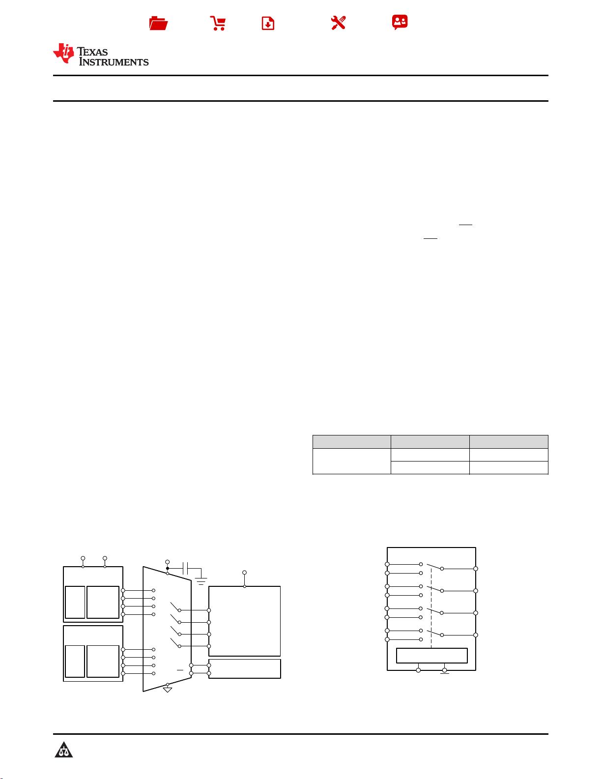
SPI / eSIM / eMMC
Device
GND
V
DD
1.8V Control Logic
From Processor / MCU
SEL
0.1µF
EN
S1B
S2B
S3B
S4B
Processor / MCU /
Ext ernal Hea der #2
S1A
S2A
S3A
S4A
Processor / MCU /
Ext ernal Hea der #1
MISO / CMD / GPIO
MOSI / CLK / GPIO
SCLK / DAT0 / GPIO
SS / DAT1 / GPIO
PORT
DEBUG,
SPI, GPIO
1.8V
Logic
I/O
PORT
DEBUG,
SPI, GPIO
1.8V
Logic
I/O
V
I/O
V
DD
D4
D3
D2
D1
V
DD
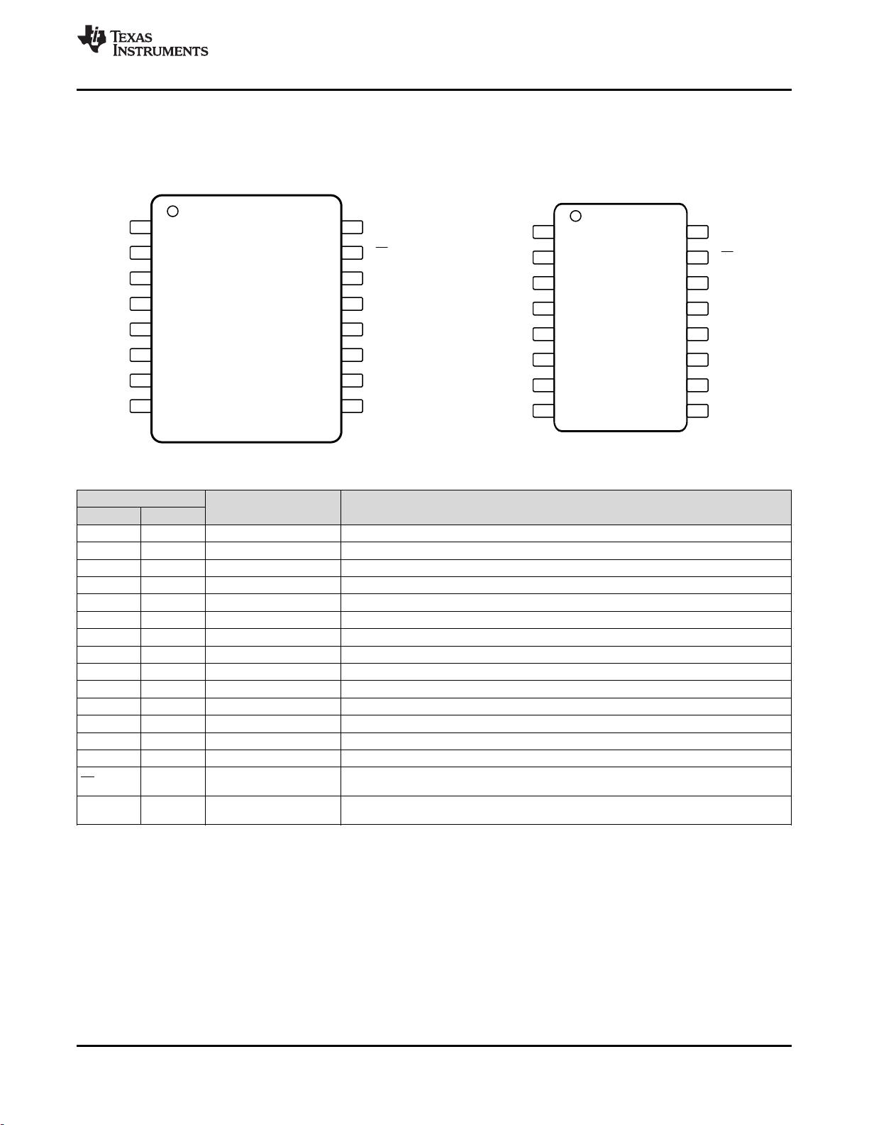
SN325 7-Q1
SEL
S1A
D1
S1B
S2A
S2B
S3A
S3B
S4A
S4B
EN
LOGIC CONTRO L*
D2
D3
D4
*Internal 6MOPull-Down on Logic Pins
Product
Folder
Order
Now
Technical
Documents
Tools &
Software
Support &
Community
本文档旨在为方便起见,提供有关 TI 产品中文版本的信息,以确认产品的概要。 有关适用的官方英文版本的最新信息,请访问 www.ti.com,其内容始终优先。 TI 不保证翻译的准确
性和有效性。 在实际设计之前,请务必参考最新版本的英文版本。
English Data Sheet: SCDS411
SN3257-Q1
ZHCSK05B –JULY 2019–REVISED JANUARY 2020
具具有有 1.8V 逻逻辑辑的的 SN3257-Q1 5V 低低传传播播延延迟迟、、2:1 (SPDT) 4 通通道道开开关关
1
1 特特性性
1
• 符合汽车应用的 AEC-Q100
– 温度等级 1:-40°C 至 +125°C,T
A
• 宽电源范围:1.5V 至 5.5V
• 低传播延迟:78ps
• 低导通电阻:5Ω
• 高带宽:1.2GHz
• 双向信号路径
• 支持超出电源电压范围的输入电压
• 兼容 1.8V 逻辑
• 逻辑引脚上的集成下拉电阻器
• 失效防护逻辑
• 高达 3.6V 信号的关断保护
2 应应用用
• SPI 多路复用
• I2S 多路复用
• eSIM 多路复用
• eMMC 多路复用
• 闪存存储器共享
• 电池管理系统 (BMS)
• 远程信息处理控制单元 (TCU)
• 智能远程信息处理网关
• 后座娱乐系统
• 数字驾驶舱处理单元
• 汽车音响主机
• 汽车导航
• ADAS 域控制器
• 环视系统 ECU
• 板载充电器 (OBC) 和无线充电器
3 说说明明
SN3257-Q1 是一款汽车级互补金属氧化物半导体
(CMOS) 开关,支持高速信号,具有低传播延迟。
SN3257-Q1 提供具有 4 个通道的 2:1 (SPDT) 开关配
置,非常适合 SPI 和 I2S 等各通道协议。此器件可在
源极(SxA、SxB)和漏极 (Dx) 引脚上支持双向模拟
和数字信号,并且能够传递高于电源电压(最高 V
DD
x
2)的信号,最大输入和输出电压为 5.5V。
SN3257-Q1 具有一个低电平有效 EN 引脚,用于同时
启用和禁用所有通道。当 EN 引脚为低电平时,会根据
SEL 引脚的状态选择两个开关路径之一。
SN3257-Q1 的信号路径上高达 3.6V 的关断保护功能
可在移除电源电压 (V
DD
= 0V) 时提供隔离。如果没有
该保护功能,开关可通过内部 ESD 二极管为电源轨进
行反向供电,从而对系统造成潜在损坏。
失效防护逻辑电路允许在施加电源引脚上的电压之前,
先施加逻辑控制引脚上的电压,从而保护器件免受潜在
的损害。两个逻辑控制输入都具有兼容 1.8V 逻辑的阈
值,可确保 TTL 和 CMOS 逻辑兼容性。逻辑引脚上带
有集成下拉电阻器,无需外部组件,可减小系统尺寸、
降低系统成本。
器器件件信信息息
(1)
器器件件型型号号 封封装装 封封装装尺尺寸寸((标标称称值值))
SN3257-Q1
TSSOP (16) 5.00mm × 4.40mm
SOT-23-THIN (16) 4.20mm x 2.00mm
(1) 如需了解所有可用封装,请参阅数据表末尾的封装选项附录。
应应用用示示例例 方方框框图图

剩余36页未读,继续阅读
资源评论


