没有合适的资源?快使用搜索试试~ 我知道了~
资源推荐
资源详情
资源评论


B
A
(9 ) 12
(8 ) 11
R
D
2 (1)
5 (4)
RE
DE
3 (2)
4 (3)
Y
Z
(7 ) 10
(
6
) 9
B
A
Y
Z
R
D
2
3
8
7
6
5
A
B
7
6
R
D
1
4
RE
DE
2
3
Product
Folder
Order
Now
Technical
Documents
Tools &
Software
Support &
Community
本文档旨在为方便起见,提供有关 TI 产品中文版本的信息,以确认产品的概要。 有关适用的官方英文版本的最新信息,请访问 www.ti.com,其内容始终优先。 TI 不保证翻译的准确
性和有效性。 在实际设计之前,请务必参考最新版本的英文版本。
English Data Sheet: SLLSEV1
THVD1510
,
THVD1512
THVD1550
,
THVD1551
,
THVD1552
ZHCSGQ1C –SEPTEMBER 2017–REVISED DECEMBER 2018
具具有有 ±18kV IEC ESD 保保护护功功能能的的 THVD15xx 5V RS-485 收收发发器器
1
1 特特性性
1
• 符合或超过 TIA/EIA-485A 标准要求
• 4.5V 至 5.5V 电源电压
• 集成总线 I/O 保护
– ±30kV HBM ESD
– ±18kV IEC 61000-4-2 ESD 接触放电
– ±25kV IEC 61000-4-2 ESD 空气间隙放电
– ±4kV IEC 61000-4-4 电气快速瞬变
• 扩展级运行共模:± 15V
• 低 EMI 500kbps 和 50Mbps 数据速率
• 扩展温度范围:-40°C 至 125°C
• 用于噪声抑制的大接收器滞后
• 低功耗
– 低待机电源电流:小于 1µA
– 运行期间的电流:< 1mA
• 适用于热插拔功能的无干扰加电/断电
• 开路、短路和空闲总线失效防护
• 1/8 单位负载选项(多达 256 个总线节点)
• 小尺寸 VSSOP 封装(可节省布板空间)或 SOIC
封装(可实现快插兼容性)
2 应应用用
• 电机驱动器
• 工厂自动化与控制
• 电网基础设施
• 楼宇自动化
• HVAC 系统
• 视频监控
• 过程分析
• 电信基础设施
3 说说明明
THVD15xx 是一系列抗噪 RS-485/RS-422 收发器,专
用于在恶劣的工业环境中运行。这些器件的总线引脚可
耐受高级别的 IEC 电气快速瞬变 (EFT) 和 IEC 静电放
电 (ESD) 事件,从而无需使用其他系统级保护组件。
每个器件由 5V 单电源供电。该系列中的器件具有扩展
共模电压范围,因此这些器件适用于长电缆上的 多点
应用。
THVD15xx 系列器件采用小型 VSSOP 封装,适用于
空间受限的 应用。这些器件在自然通风环境下的额定
温度范围为 –40°C 至 125°C。
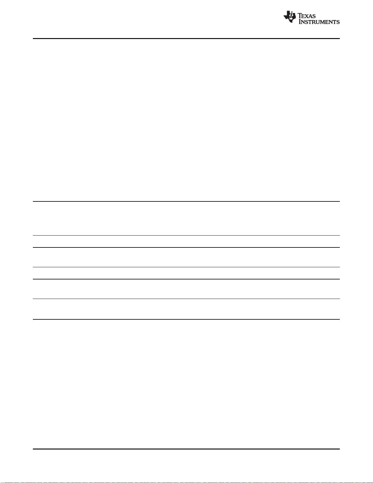
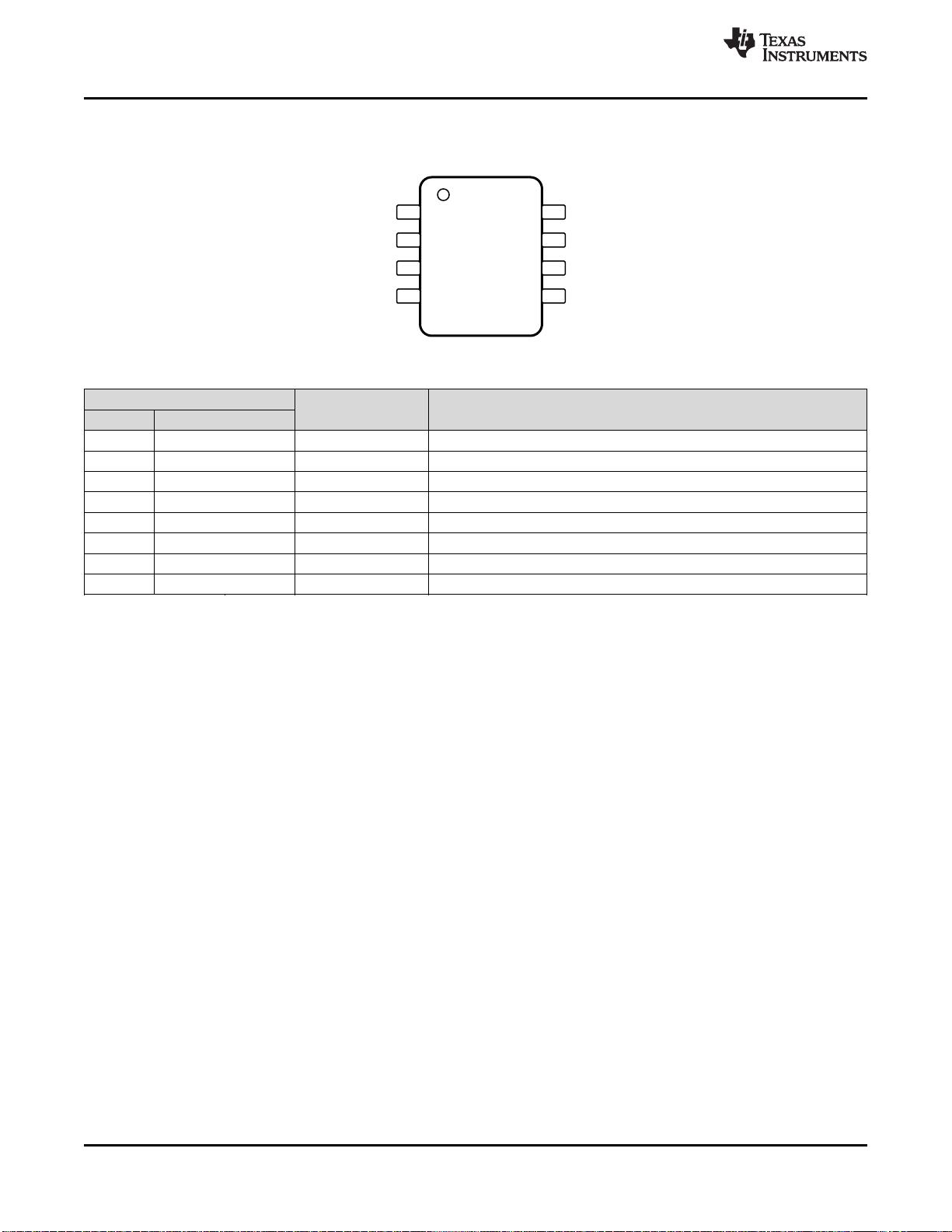
器器件件信信息息
(1)
器器件件型型号号 封封装装 封封装装尺尺寸寸((标标称称值值))
THVD1510
THVD1550
VSSOP (8) 3.00mm × 3.00mm
SOIC (8) 4.90mm × 3.91mm
THVD1551 VSSOP (8) 3.00mm × 3.00mm
THVD1512 VSSOP (10) 3.00mm × 3.00mm
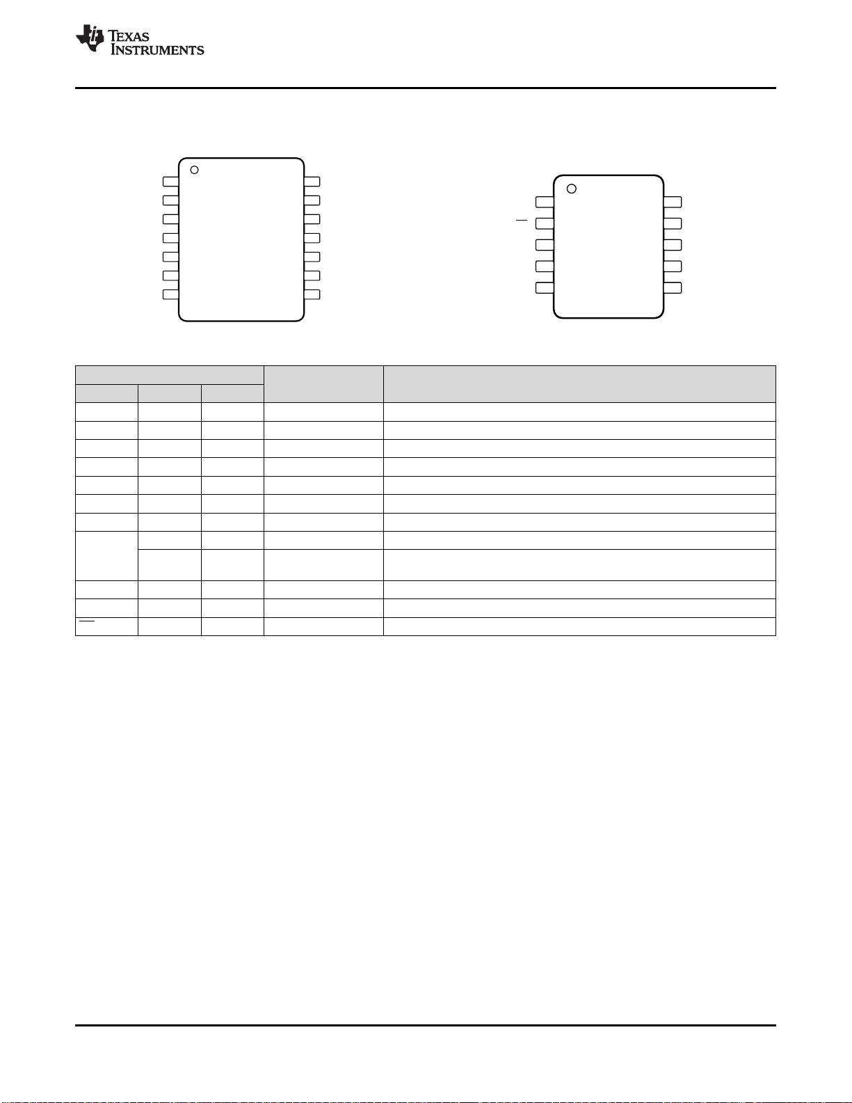
THVD1552
VSSOP (10) 3.00mm × 3.00mm
SOIC (14) 8.65mm × 3.91mm
(1) 如需了解所有可用封装,请参阅产品说明书末尾的可订购产品
附录。
THVD1510 和和 THVD1550 简简化化原原理理图图
THVD1551 简简化化原原理理图图
THVD1512 和和 THVD1552 简简化化原原理理图图

2
THVD1510
,
THVD1512
THVD1550
,
THVD1551
,
THVD1552
ZHCSGQ1C –SEPTEMBER 2017 –REVISED DECEMBER 2018
www.ti.com.cn
Copyright © 2017–2018, Texas Instruments Incorporated
目目录录
1 特特性性.......................................................................... 1
2 应应用用.......................................................................... 1
3 说说明明.......................................................................... 1
4 修修订订历历史史记记录录 ........................................................... 2
5 Device Comparison Table..................................... 3
6 Pin Configuration and Functions......................... 3
7 Specifications......................................................... 6
7.1 Absolute Maximum Ratings ...................................... 6
7.2 ESD Ratings ............................................................ 6
7.3 Recommended Operating Conditions....................... 7
7.4 Thermal Information.................................................. 7
7.5 Power Dissipation ..................................................... 7
7.6 Electrical Characteristics........................................... 8
7.7 Switching Characteristics.......................................... 9
7.8 Switching Characteristics.......................................... 9
7.9 Typical Characteristics............................................ 10
8 Parameter Measurement Information ................ 11
9 Detailed Description............................................ 14
9.1 Overview ................................................................. 14
9.2 Functional Block Diagrams ..................................... 14
9.3 Feature Description................................................. 14
9.4 Device Functional Modes........................................ 15
10 Application and Implementation........................ 18
10.1 Application Information...................................... 18
10.2 Typical Application ............................................... 18
11 Power Supply Recommendations ..................... 24
12 Layout................................................................... 25
12.1 Layout Guidelines ................................................. 25
12.2 Layout Example .................................................... 25
13 器器件件和和文文档档支支持持 ..................................................... 26
13.1 器件支持................................................................ 26
13.2 第三方产品免责声明.............................................. 26
13.3 相关链接................................................................ 26
13.4 接收文档更新通知 ................................................. 26
13.5 社区资源................................................................ 26
13.6 商标 ....................................................................... 26
13.7 静电放电警告......................................................... 26
13.8 术语表 ................................................................... 26
14 机机械械、、封封装装和和可可订订购购信信息息....................................... 27
4 修修订订历历史史记记录录
Changes from Revision B (July 2018) to Revision C Page
• Changed the Description of pins 13 and 14 in the Pin Functions table for THVD1512, THVD1552 D package................... 5
Changes from Revision A (January 2018) to Revision B Page
• Added T
SD
to the Electrical Characteristics table ................................................................................................................... 8
Changes from Original (September 2017) to Revision A Page
• Changed the Machine model (MM) value From: ±400 To: ±200 in the ESD Ratings............................................................ 6
• Changed the V
OH
MIN value From: 2.4 V To: 4 V in the Electrical Characteristics table ..................................................... 8

Not to scale
1R 8 VCC
2/RE 7 B
3DE 6 A
4D 5 GND
Not to scale
1R 8 VCC
2/RE 7 B
3DE 6 A
4D 5 GND
3
THVD1510
,
THVD1512
THVD1550
,
THVD1551
,
THVD1552
www.ti.com.cn
ZHCSGQ1C –SEPTEMBER 2017 –REVISED DECEMBER 2018
Copyright © 2017–2018, Texas Instruments Incorporated
5 Device Comparison Table
PART NUMBER DUPLEX ENABLES SIGNALING RATE NODES
THVD1512 Full DE, RE
up to 500 kbps 256
THVD1510 Half DE, RE
THVD1552 Full DE, RE
up to 50 Mbps 196THVD1551 Full None
THVD1550 Half DE, RE
6 Pin Configuration and Functions
THVD1510, THVD1550 Devices
8-Pin D Package (SOIC)
Top View
THVD1510, THVD1550 Devices
8-Pin DGK Package (VSSOP)
Top View
Pin Functions
PIN
I/O DESCRIPTION
NAME D DGK
A 6 6 Bus input/output Bus I/O port, A (complementary to B)
B 7 7 Bus input/output Bus I/O port, B (complementary to A)
D 4 4 Digital input Driver data input
DE 3 3 Digital input Driver enable, active high (2 MΩ internal pull-down)
GND 5 5 Ground Device ground
R 1 1 Digital output Receive data output
V
CC
8 8 Power 5-V supply
RE 2 2 Digital input Receiver enable, active low (2 MΩ internal pull-up)

Not to scale
1VCC 8 A
2R 7 B
3D 6 Z
4GND 5 Y
4
THVD1510
,
THVD1512
THVD1550
,
THVD1551
,
THVD1552
ZHCSGQ1C –SEPTEMBER 2017 –REVISED DECEMBER 2018
www.ti.com.cn
Copyright © 2017–2018, Texas Instruments Incorporated
THVD1551 Device
8-Pin DGK Package (VSSOP)
Top View
Pin Functions
PIN
I/O DESCRIPTION
NAME DGK
A 8 Bus input Bus input, A (complementary to B)
B 7 Bus input Bus input, B (complementary to A)
D 3 Digital input Driver data input
GND 4 Ground Device ground
R 2 Digital output Receive data output
V
CC
1 Power 5-V supply
Y 5 Bus output Bus output, Y (complementary to Z)
Z 6 Bus output Bus output, Z (complementary to Y)

Not to scale
1NC 14 VCC
2R 13 VCC
3/RE 12 A
4DE 11 B
5D 10 Z
6GND 9 Y
7GND 8 NC
Not to scale
1R 10 VCC
2RE 9 A
3DE 8 B
4D 7 Z
5GND 6 Y
5
THVD1510
,
THVD1512
THVD1550
,
THVD1551
,
THVD1552
www.ti.com.cn
ZHCSGQ1C –SEPTEMBER 2017 –REVISED DECEMBER 2018
Copyright © 2017–2018, Texas Instruments Incorporated
THVD1552 Device
14-Pin D Package (SOIC)
Top View
THVD1512, THVD1552 Devices
10-Pin DGS Package (VSSOP)
Top View
(1) These pins are internally connected
Pin Functions
PIN
I/O DESCRIPTION
NAME D DGS
A 12 9 Bus input Bus input, A (complementary to B)
B 11 8 Bus input Bus input, B (complementary to A)
D 5 4 Digital input Driver data input
DE 4 3 Digital input Driver enable, active high (2 MΩ internal pull-down)
GND 6, 7
(1)
5 Ground Device ground
NC 1, 8 — — Internally not connected
R 2 1 Digital output Receive data output
V
CC
— 10 Power 5-V supply.
13, 14 — Power
5-V supply. These pins are not connected together internally, so power must
be applied to both.
Y 9 6 Bus output Bus output, Y (Complementary to Z)
Z 10 7 Bus output Bus output, Z (Complementary to Y)
RE 3 2 Digital input Receiver enable, active low (2 MΩ internal pull-up)
剩余40页未读,继续阅读
资源评论

不觉明了
- 粉丝: 701
- 资源: 4046

上传资源 快速赚钱
我的内容管理 收起
我的资源 快来上传第一个资源
我的收益
登录查看自己的收益我的积分 登录查看自己的积分
我的C币 登录后查看C币余额
我的收藏
我的下载
下载帮助

会员权益专享
安全验证
文档复制为VIP权益,开通VIP直接复制
