没有合适的资源?快使用搜索试试~ 我知道了~
TI-TMS44100.pdf
需积分: 0 0 下载量 182 浏览量
2022-12-10
23:05:29
上传
评论 4
收藏 384KB PDF 举报
温馨提示
![preview](https://dl-preview.csdnimg.cn/87265393/0001-0002cad8a8580365132fd29b09d6713c_thumbnail.jpeg)
![preview-icon](https://csdnimg.cn/release/downloadcmsfe/public/img/scale.ab9e0183.png)
试读
25页
TI-TMS44100.pdf
资源推荐
资源详情
资源评论
![](https://csdnimg.cn/release/download_crawler_static/87265393/bg1.jpg)
TMS44100, TMS44100P, TMS46100, TMS46100P
4194304-WORD BY 1-BIT
DYNAMIC RANDOM-ACCESS MEMORIES
SMHS561A – MARCH 1995 – REVISED JUNE 1995
1
POST OFFICE BOX 1443 • HOUSTON, TEXAS 77251–1443
D
Organization...4194304 × 1
D
Single 5 V Power Supply, for TMS44100/P
(±10% Tolerance)
D
Single 3.3 V Power Supply, for TMS46100/P
(±10% Tolerance)
D
Low Power Dissipation (TMS46100P only)
– 200-µA CMOS Standby
– 200-µA Self Refresh
– 300-µA Extended-Refresh Battery
Backup
D
Performance Ranges:
ACCESS ACCESS ACCESS READ
TIME TIME TIME OR WRITE
(t
RAC
)(t
CAC
)(t
AA
) CYCLE
(MAX) (MAX) (MAX) (MIN)
’4x100/P-60 60 ns 15 ns 30 ns 110 ns
’4x100/P-70 70 ns 18 ns 35 ns 130 ns
’4x100/P-80 80 ns 20 ns 40 ns 150 ns
D
Enhanced Page-Mode Operation for Faster
Memory Access
D
CAS-Before-RAS (CBR) Refresh
D
Long Refresh Period
– 1024-Cycle Refresh in 16 ms
– 128 ms (Max) for Low-Power,
Self-Refresh Version (TMS4x100P)
D
3-State Unlatched Output
D
Texas Instruments EPIC CMOS Process
D
Operating Free-Air Temperature Range
0°C to 70°C
DEVICE
POWER
SUPPLY
SELF-REFRESH
BATTERY
BACKUP
REFRESH
CYCLES
TMS44100 5 V — 1024 in 16 ms
TMS44100P 5 V YES 1024 in 128 ms
TMS46100 3.3 V — 1024 in 16 ms
TMS46100P 3.3 V YES 1024 in 128 ms
These devices feature maximum RAS access times of 60 ns, 70 ns, and 80 ns. All addresses and data-in lines
are latched on chip to simplify system design. Data out is unlatched to allow greater system flexibility.
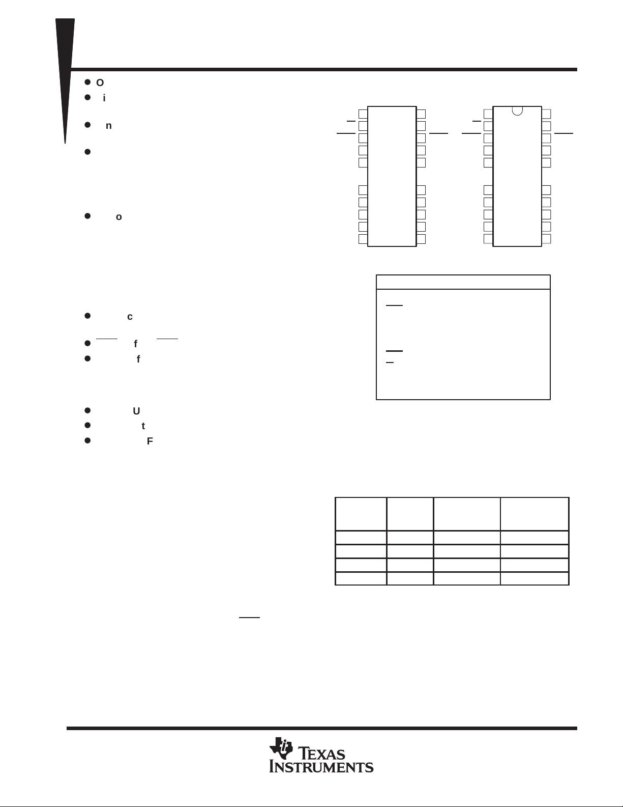
The TMS4x100 and TMS4x100P are offered in a 20-/26-lead plastic surface-mount small-outline (TSOP)
package (DGA suffix) and a 300-mil 20-/26-lead plastic surface-mount SOJ package (DJ suffix). Both packages
are characterized for operation from 0°C to 70°C.
ADVANCE INFORMATION concerns new products in the sampling or
preproduction phase of development. Characteristic data and other
specifications are subject to change without notice.
PIN NOMENCLATURE
A0–A10 Address Inputs
CAS
Column-Address Strobe
D Data In
NC No Connection
Q Data Out
RAS
Row-Address Strobe
W
Write Enable
V
CC
5-V or 3.3-V Supply
V
SS
Ground
DJ PACKAGE
(TOP VIEW)
V
SS
Q
CAS
NC
A9
A8
A7
A6
A5
A4
26
25
24
23
22
18
17
16
15
14
1
2
3
4
5
9
10
11
12
13
DGA PACKAGE
(TOP VIEW)
D
W
RAS
NC
A10
A0
A1
A2
A3
V
CC
V
SS
Q
CAS
NC
A9
A8
A7
A6
A5
A4
26
25
24
23
22
18
17
16
15
14
1
2
3
4
5
9
10
11
12
13
D
W
RAS
NC
A10
A0
A1
A2
A3
V
CC
EPIC is a trademark of Texas Instruments Incorporated.
ADVANCE INFORMATION
description
The TMS4x100 series are high-speed,
4194304-bit dynamic random-access memories,
organized as 4194304 words of one bit each. The
TMS4x100P series are high-speed, low-power,
self-refresh with extended-refresh, 4194304-bit
dynamic random-access memories, organized as
4194304 words of one bit each. Both series
employ state-of-the-art EPIC
(Enhanced
Performance Implanted CMOS) technology for
high performance, reliability, and low voltage.
Copyright 1995, Texas Instruments Incorporated
![](https://csdnimg.cn/release/download_crawler_static/87265393/bg2.jpg)
TMS44100, TMS44100P, TMS46100, TMS46100P
4194304-WORD BY 1-BIT
DYNAMIC RANDOM-ACCESS MEMORIES
SMHS561A – MARCH 1995 – REVISED JUNE 1995
2
POST OFFICE BOX 1443 • HOUSTON, TEXAS 77251–1443
logic symbol
†
A0
A1
A2
A3
A4
A5
A6
A7
A8
A10
RAS
CAS
W
D
9
10
11
12
14
15
16
17
18
5
3
24
2
1
30D11/21D0
31D21/21D10
C30 [ROW]
G33 [REFRESH ROW]
34 [PWR DWN]
C31 [COL]
G34
33C32
33,31D 34
EN
A, 32D
A
0
4 194 303
RAM 4096K × 1
&
A∇ Q
25
A9
22
†
This symbol is in accordance with ANSI/IEEE Std 91-1984 and IEC Publication 617-12.
functional block diagram
A0
A1
A10
16
3
8
10
10
16
16
3
Timing and Control
Column-
Address
Buffers
Row-
Address
Buffers
I/O
Buffers
1 of 16
Selection
Data-
In
Reg.
Data-
Out
Reg.
Column Decode
Sense Amplifiers
R
o
w
D
e
c
o
d
e
16
128K Array
128K Array
128K Array
128K Array
128K Array
128K Array
D
RAS
CAS W
Q
ADVANCE INFORMATION
![](https://csdnimg.cn/release/download_crawler_static/87265393/bg3.jpg)
TMS44100, TMS44100P, TMS46100, TMS46100P
4194304-WORD BY 1-BIT
DYNAMIC RANDOM-ACCESS MEMORIES
SMHS561A – MARCH 1995 – REVISED JUNE 1995
3
POST OFFICE BOX 1443 • HOUSTON, TEXAS 77251–1443
operation
enhanced page mode
Enhanced page-mode operation allows faster memory access by keeping the same row address while selecting
random column addresses. The time for row-address setup and hold and address multiplex is eliminated. The
maximum number of columns that can be accessed is determined by the maximum RAS
low time and the CAS
page cycle time used.
Unlike conventional page-mode DRAMs, the column-address buffers in this device are activated on the falling
edge of RAS
. The buffers act as transparent or flow-through latches while CAS is high. The falling edge of CAS
latches the column addresses. This feature allows the TMS4x100 to operate at a higher data bandwidth than
conventional page-mode parts because data retrieval begins as soon as the column address is valid rather than
when CAS
transitions low. This performance improvement is referred to as enhanced page mode. A valid
column address can be presented immediately after row-address hold time has been satisfied, usually well in
advance of the falling edge of CAS
. In this case, data is obtained after t
CAC
max (access time from CAS low),
if t
AA
max (access time from column address) has been satisfied. If column addresses for the next cycle are
valid at the time CAS
goes high, access time for the next cycle is determined by the later occurrence of t
CAC
or t
CPA
(access time from rising edge of CAS).
address (A0–A10)
Twenty-two address bits are required to decode 1 of 4194304 storage cell locations. Eleven row-address bits
are set up on inputs A0 through A10 and latched onto the chip by the row-address strobe (RAS
). The eleven
column-address bits are set up on A0 through A10 and latched onto the chip by the column-address strobe
(CAS
). All addresses must be stable on or before the falling edges of RAS and CAS. RAS is similar to a chip
enable in that it activates the sense amplifiers as well as the row decoder. CAS
is used as a chip select, activating
the output buffer, as well as latching the address bits into the column-address buffer.
write enable (W
)
The read or write mode is selected through the write-enable (W
) input. A logic high on W selects the read mode
and a logic low selects the write mode. W
can be driven from standard TTL circuits (TMS44100/P) or
low-voltage TTL circuits (TMS46100/P) without a pullup resistor. The data input is disabled when the read mode
is selected. When W
goes low prior to CAS (early write), data out remains in the high-impedance state for the
entire cycle, permitting common I/O operation.
data in (D)
Data is written during a write or read-write cycle. Depending on the mode of operation, the falling edge of CAS
or W strobes data into the on-chip data latch. In an early-write cycle, W is brought low prior to CAS and the data
is strobed in by CAS
with setup and hold times referenced to this signal. In a delayed-write or read-write cycle,
CAS
is already low and the data is strobed in by W with setup and hold times referenced to this signal.
data out (Q)
Data out is the same polarity as data in. The output is in the high-impedance (floating) state until CAS
is brought
low. In a read cycle, the output becomes valid after the access time interval t
CAC
(which begins with the negative
transition of CAS
) as long as t
RAC
and t
AA
are satisfied. The output becomes valid after the access time has
elapsed and remains valid while CAS
is low; CAS going high returns it to the high-impedance state. In a
delayed-write or read-write cycle, the output follows the sequence for the read cycle.
ADVANCE INFORMATION
![](https://csdnimg.cn/release/download_crawler_static/87265393/bg4.jpg)
TMS44100, TMS44100P, TMS46100, TMS46100P
4194304-WORD BY 1-BIT
DYNAMIC RANDOM-ACCESS MEMORIES
SMHS561A – MARCH 1995 – REVISED JUNE 1995
4
POST OFFICE BOX 1443 • HOUSTON, TEXAS 77251–1443
refresh
A refresh operation must be performed at least once every 16 ms (128 ms for TMS4x100P) to retain data. This
can be achieved by strobing each of the 1024 rows (A0–A9). A normal read or write cycle refreshes all bits in
each row that is selected. A RAS
-only operation can be used by holding CAS at the high (inactive) level,
conserving power as the output buffer remains in the high-impedance state. Externally generated addresses
must be used for a RAS
-only refresh. Hidden refresh can be performed while maintaining valid data at the
output. This is accomplished by holding CAS
at V
IL
after a read operation and cycling RAS after a specified
precharge period, similar to a RAS
-only refresh cycle. The external address is ignored during the hidden-refresh
cycle.
CAS
-before-RAS (CBR) refresh
CBR refresh is utilized by bringing CAS
low earlier than RAS (see parameter t
CSR
) and holding it low after RAS
falls (see parameter t
CHR
). For successive CBR refresh cycles, CAS can remain low while cycling RAS. The
external address is ignored and the refresh address is generated internally.
A low-power battery-backup refresh mode that requires less than 300-µA (TMS46100P) or 500-µA
(TMS44100P) refresh current is available on the low-power devices. Data integrity is maintained using CBR
refresh with a period of 125 µs while holding RAS
low for less than 1 µs. To minimize current consumption, all
input levels need to be at CMOS levels (V
IL
≤ 0.2 V, V
IH
≥ V
CC
– 0.2 V).
self refresh
The self-refresh mode is entered by dropping CAS
low prior to RAS going low. CAS and RAS are both held low
for a minimum of 100 µs. The chip is then refreshed by an on-board oscillator. No external address is required
because the CBR counter is used to keep track of the address. To exit the self-refresh mode, both RAS
and CAS
are brought high to satisfy t
CHS
. Upon exiting the self-refresh mode, a burst refresh (refresh a full set of row
addresses) must be executed before continuing with normal operation. This ensures the DRAM is fully
refreshed.
power up
To achieve proper device operation, an initial pause of 200 µs followed by a minimum of eight initialization cycles
is required after full V
CC
level is achieved. These eight initialization cycles must include at least one refresh
(RAS
-only or CBR) cycle.
test mode
An industry-standard design-for-test (DFT) mode is incorporated in the TMS4x100 and TMS4x100P. A CBR
cycle with W
low (WCBR) cycle is used to enter the test mode. In the test mode, data is written into and read
from eight sections of the array in parallel. Data is compared upon reading and if all bits are equal, the data-out
terminal goes high. If any one bit is different, the data-out terminal goes low. Any combination of read, write,
read-write, or page-mode cycles can be used in the test mode. The test-mode function reduces test times by
enabling the 4-Mbit DRAM to be tested as if it were a 512K DRAM, where row address 10, column address 10,
and column address 0 are not used. A RAS
-only or CBR refresh cycle is used to exit the DFT mode.
ADVANCE INFORMATION
![](https://csdnimg.cn/release/download_crawler_static/87265393/bg5.jpg)
TMS44100, TMS44100P, TMS46100, TMS46100P
4194304-WORD BY 1-BIT
DYNAMIC RANDOM-ACCESS MEMORIES
SMHS561A – MARCH 1995 – REVISED JUNE 1995
5
POST OFFICE BOX 1443 • HOUSTON, TEXAS 77251–1443
test mode (continued)
Test-Mode Cycle
Entry Cycle
Exit Cycle
Normal
Mode
RAS
CAS
W
†
The states of W
, data in, and address are defined by the type of cycle used during test mode.
absolute maximum ratings over operating free-air temperature range (unless otherwise noted)
‡
Supply voltage range, V
CC
: TMS44100, TMS44100P – 1 V to 7 V. . . . . . . . . . . . . . . . . . . . . . . . .
TMS46100, TMS46100P – 0.5 V to 4.6 V. . . . . . . . . . . . . . . . . . . . . .
Voltage range on any pin (see Note 1): TMS44100, TMS44100P – 1 V to 7 V. . . . . . . . . . . . . . . . . . . . . . . .
TMS46100, TMS46100P – 0.5 V to 4.6 V. . . . . . . . . . . . . . . . . . . . . .
Short-circuit output current 50 mA. . . . . . . . . . . . . . . . . . . . . . . . . . . . . . . . . . . . . . . . . . . . . . . . . . . . . . . . . . . . . . . .
Power dissipation 1 W. . . . . . . . . . . . . . . . . . . . . . . . . . . . . . . . . . . . . . . . . . . . . . . . . . . . . . . . . . . . . . . . . . . . . . . . . .
Operating free-air temperature range, T
A
0°C to 70°C. . . . . . . . . . . . . . . . . . . . . . . . . . . . . . . . . . . . . . . . . . . . . .
Storage temperature range, T
stg
–55°C to 150°C. . . . . . . . . . . . . . . . . . . . . . . . . . . . . . . . . . . . . . . . . . . . . . . . . .
‡
Stresses beyond those listed under “absolute maximum ratings” may cause permanent damage to the device. These are stress ratings only, and
functional operation of the device at these or any other conditions beyond those indicated under “recommended operating conditions” is not
implied. Exposure to absolute-maximum-rated conditions for extended periods may affect device reliability.
NOTE 1: All voltage values are with respect to V
SS
.
recommended operating conditions
TMS44100/P TMS46100/P
UNIT
MIN NOM MAX MIN NOM MAX
UNIT
V
CC
Supply voltage 4.5 5 5.5 3 3.3 3.6 V
V
IH
High-level input voltage 2.4 6.5 2 V
CC
+ 0.3 V
V
IL
Low-level input voltage (see Note 2) –1 0.8 – 0.3 0.8 V
T
A
Operating free-air temperature 0 70 0 70
°C
NOTE 2: The algebraic convention, where the more negative (less positive) limit is designated as minimum, is used for logic-voltage levels only.
ADVANCE INFORMATION
剩余24页未读,继续阅读
资源评论
![avatar-default](https://csdnimg.cn/release/downloadcmsfe/public/img/lazyLogo2.1882d7f4.png)
![avatar](https://profile-avatar.csdnimg.cn/107303f5121d47e49d12d0a9ae68af10_weixin_54787054.jpg!1)
不觉明了
- 粉丝: 3233
- 资源: 5614
上传资源 快速赚钱
我的内容管理 展开
我的资源 快来上传第一个资源
我的收益
登录查看自己的收益我的积分 登录查看自己的积分
我的C币 登录后查看C币余额
我的收藏
我的下载
下载帮助
![voice](https://csdnimg.cn/release/downloadcmsfe/public/img/voice.245cc511.png)
![center-task](https://csdnimg.cn/release/downloadcmsfe/public/img/center-task.c2eda91a.png)
安全验证
文档复制为VIP权益,开通VIP直接复制
![dialog-icon](https://csdnimg.cn/release/downloadcmsfe/public/img/green-success.6a4acb44.png)