没有合适的资源?快使用搜索试试~ 我知道了~
TI-TMS416160.pdf
需积分: 0 0 下载量 142 浏览量
2022-12-10
23:07:02
上传
评论 4
收藏 414KB PDF 举报
温馨提示
![preview](https://dl-preview.csdnimg.cn/87265410/0001-f083f5d1a29d91b6a4c2368d6d6242dd_thumbnail.jpeg)
![preview-icon](https://csdnimg.cn/release/downloadcmsfe/public/img/scale.ab9e0183.png)
试读
28页
TI-TMS416160.pdf
资源详情
资源评论
![](https://csdnimg.cn/release/download_crawler_static/87265410/bg1.jpg)
TMS416160, TMS416160P, TMS418160, TMS418160P
TMS426160, TMS426160P, TMS428160, TMS428160P
1048576-WORD BY 16-BIT HIGH-SPEED DRAMS
SMKS160C – MAY 1995–REVISED NOVEMBER 1995
1
POST OFFICE BOX 1443 • HOUSTON, TEXAS 77251–1443
D
Organization...1048576 × 16
D
Single Power Supply (5 V or 3.3 V)
D
Performance Ranges:
ACCESS ACCESS ACCESS READ OR
TIME TIME TIME WRITE
t
RAC
t
CAC
t
AA
CYCLE
MAX MAX MAX MIN
’4xx160/P-60 60 ns 15 ns 30 ns 110 ns
’4xx160/P-70 70 ns 18 ns 35 ns 130 ns
’4xx160/P-80 80 ns 20 ns 40 ns 150 ns
D
Enhanced Page-Mode Operation With
CAS
-Before-RAS (CBR) Refresh
D
Long Refresh Period and Self-Refresh
Option (TMS4xx160P)
D
3-State Unlatched Output
D
Low Power Dissipation
D
High-Reliability Plastic 42-Lead (DZ Suffix)
400-Mil-Wide Surface-Mount (SOJ) Package
and 44/50-Lead (DGE Suffix) Surface-Mount
Thin Small-Outline Package (TSOP)
D
Operating Free-Air Temperature Range
0°C to 70°C
D
Fabricated Using the Texas Instruments
Enhanced Performance Implanted CMOS
(EPIC) Technology
AVAILABLE OPTIONS
DEVICE
POWER
SUPPLY
SELF
REFRESH,
BATTERY
BACKUP
REFRESH
CYCLES
TMS416160
TMS416160P
TMS418160
TMS418160P
TMS426160
TMS426160P
TMS428160
TMS428160P
5 V
5 V
5 V
5 V
3.3 V
3.3 V
3.3 V
3.3 V
—
Yes
—
Yes
—
Yes
—
Yes
4096 in 64 ms
4096 in 128 ms
1024 in 16 ms
1024 in 128 ms
4096 in 64 ms
4096 in 128 ms
1024 in 16 ms
1024 in 128 ms
description
The TMS4xx160 series is a set of high-speed,
16777216-bit dynamic random-access memo-
ries (DRAMs) organized as 1048576 words of 16
bits each. The TMS4xx160P series is a similar
set of high-speed, low-power, self-refresh,
16777216-bit DRAMs organized as 1048576 words of 16 bits each. Both sets employ state-of-the-art
enhanced performance implanted CMOS (EPIC) technology for high performance, reliability, and low power
at low cost.
Please be aware that an important notice concerning availability, standard warranty, and use in critical applications of
Texas Instruments semiconductor products and disclaimers thereto appears at the end of this data sheet.
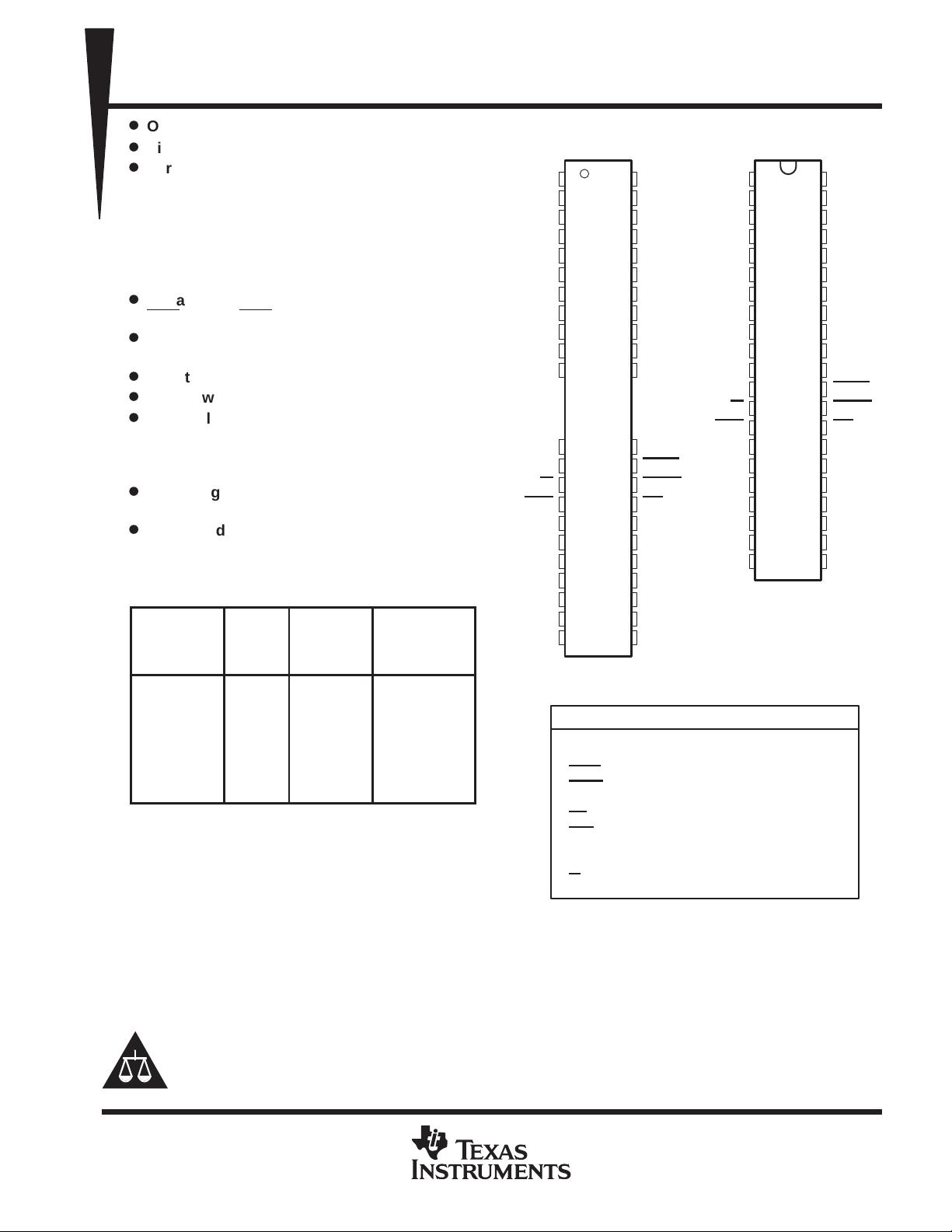
PIN NOMENCLATURE
A0– A11 Address Inputs
DQ0–DQ15 Data In/Data Out
LCAS
Lower Column-Address Strobe
UCAS
Upper Column-Address Strobe
NC No Internal Connection
OE
Output Enable
RAS
Row-Address Strobe
V
CC
5-V or 3.3-V Supply
‡
V
SS
Ground
W
Write Enable
V
SS
DQ15
DQ14
DQ13
DQ12
V
SS
DQ11
DQ10
DQ9
DQ8
NC
1
2
3
4
5
6
7
8
9
10
11
50
49
48
47
46
45
44
43
42
41
40
V
CC
DQ0
DQ1
DQ2
DQ3
V
CC
DQ4
DQ5
DQ6
DQ7
NC
NC
LCAS
UCAS
OE
A9
A8
A7
A6
A5
A4
V
SS
DGE PACKAGE
(TOP VIEW)
15
16
17
18
19
20
21
22
23
24
25
36
35
34
33
32
31
30
29
28
27
26
NC
NC
W
RAS
A11
†
A10
†
A0
A1
A2
A3
V
CC
1
2
3
4
5
6
7
8
9
10
11
12
13
14
15
16
17
18
19
20
21
42
41
40
39
38
37
36
35
34
33
32
31
30
29
28
27
26
25
24
23
22
V
CC
DQ0
DQ1
DQ2
DQ3
V
CC
DQ4
DQ5
DQ6
DQ7
NC
NC
W
RAS
A11
†
A10
†
A0
A1
A2
A3
V
CC
V
SS
DQ15
DQ14
DQ13
DQ12
V
SS
DQ11
DQ10
DQ9
DQ8
NC
LCAS
UCAS
OE
A9
A8
A7
A6
A5
A4
V
SS
DZ PACKAGE
(TOP VIEW)
‡
See Available Options Table.
†
A10 and A11 are NC for TMS4x8160 and TMS4x8160P.
EPIC is a trademark of Texas Instruments Incorporated.
PRODUCTION DATA information is current as of publication date.
Products conform to specifications per the terms of Texas Instruments
standard warranty. Production processing does not necessarily include
testing of all parameters.
Copyright 1995, Texas Instruments Incorporated
![](https://csdnimg.cn/release/download_crawler_static/87265410/bg2.jpg)
TMS416160, TMS416160P, TMS418160, TMS418160P
TMS426160, TMS426160P, TMS428160, TMS428160P
1048576-WORD BY 16-BIT HIGH-SPEED DRAMS
SMKS160C – MAY 1995– REVISED NOVEMBER 1995
2
POST OFFICE BOX 1443 • HOUSTON, TEXAS 77251–1443
description (continued)
These devices feature maximum RAS access times of 60 ns, 70 ns, and 80 ns. All addresses and data-in lines
are latched on chip to simplify system design. Data out is unlatched to allow greater system flexibility.
The TMS4xx160 and TMS4xx160P are offered in a 44/50-lead plastic surface-mount TSOP (DGE suffix) and
a 42-lead plastic surface-mount SOJ (DZ suffix) package. These packages are characterized for operation from
0°C to 70°C.
![](https://csdnimg.cn/release/download_crawler_static/87265410/bg3.jpg)
TMS416160, TMS416160P, TMS418160, TMS418160P
TMS426160, TMS426160P, TMS428160, TMS428160P
1048576-WORD BY 16-BIT HIGH-SPEED DRAMS
SMKS160C – MAY 1995– REVISED NOVEMBER 1995
3
POST OFFICE BOX 1443 • HOUSTON, TEXAS 77251–1443
logic symbol
†
3
4
5
7
8
9
10
33
34
35
38
39
40
41
36
14
31
30
2
13
29
A0
A1
A2
A3
A4
A5
A6
A7
17
18
19
20
23
24
25
26
DQ1
DQ2
DQ3
DQ4
DQ5
DQ6
DQ7
DQ8
DQ9
DQ10
DQ11
DQ12
DQ13
DQ14
DQ15
DQ0
RAS
LCAS
UCAS
W
RAM 1M × 16
C20[ROW]
G23/[REFRESH ROW]
24[PWR DWN]
C21
G24
&
23C22
A,22D
A8
27
31
C21
G34
&
31
Z31
24,25EN27
34
,25EN37
23C32
23,21D
∇26,27
A, Z26
A,32D
∇36,37
A, Z36
OE
A
0
1 048 575
A9
28
25
20D15/21D7
20D16
20D17
20D8/21D0
A10
‡
16
A11
‡
15
20D18
20D19
†
This symbol is in accordance with ANSI/IEEE Std 91-1984 and IEC Publication 617-12.
The pin numbers shown correspond to the DZ package.
‡
A10 and A11 are NC for TMS4x8160 and TMS4x8160P.
![](https://csdnimg.cn/release/download_crawler_static/87265410/bg4.jpg)
TMS416160, TMS416160P, TMS418160, TMS418160P
TMS426160, TMS426160P, TMS428160, TMS428160P
1048576-WORD BY 16-BIT HIGH-SPEED DRAMS
SMKS160C – MAY 1995– REVISED NOVEMBER 1995
4
POST OFFICE BOX 1443 • HOUSTON, TEXAS 77251–1443
functional block diagrams (TMS4x6160/P)
A0
A1
A7
32
16
16
Timing and Control
Column-
Address
Buffers
Row-
Address
Buffers
I/O
Buffers
Data-
In
Reg.
Data-
Out
Reg.
Column Decode
Sense Amplifiers
R
o
w
D
e
c
o
d
e
256K Array
256K Array
256K Array
256K Array
256K Array
256K Array
DQ0–DQ15
RAS
UCAS W OELCAS
16 of 32
Selection
32
A8–
A11
4
8
12
12
32
32
(a) TMS4x6160, TMS4x6160P
functional block diagram (TMS4x8160/P)
A0
A1
A9
32
16
16
Timing and Control
Column-
Address
Buffers
Row-
Address
Buffers
I/O
Buffers
Data-
In
Reg.
Data-
Out
Reg.
Column Decode
Sense Amplifiers
R
o
w
D
e
c
o
d
e
256K Array
256K Array
256K Array
256K Array
256K Array
256K Array
DQ0–DQ15
RAS
UCAS W OELCAS
16 of 32
Selection
32
10
10
10
32
32
(b) TMS4x8160, TMS4x8160P
![](https://csdnimg.cn/release/download_crawler_static/87265410/bg5.jpg)
TMS416160, TMS416160P, TMS418160, TMS418160P
TMS426160, TMS426160P, TMS428160, TMS428160P
1048576-WORD BY 16-BIT HIGH-SPEED DRAMS
SMKS160C – MAY 1995– REVISED NOVEMBER 1995
5
POST OFFICE BOX 1443 • HOUSTON, TEXAS 77251–1443
operation
dual CAS
Two CAS pins (LCAS and UCAS) are provided to give independent control of the 16 data-I/O pins
(DQ0–DQ15), with LCAS
corresponding to DQ0–DQ7 and UCAS corresponding to DQ8–DQ15. For read or
write cycles, the column address is latched on the first xCAS
falling edge. Each xCAS going low enables its
corresponding DQx pin with data associated with the column address latched on the first falling xCAS
edge.
All address setup and hold parameters are referenced to the first falling xCAS
edge.The delay time from xCAS
low to valid data out (see parameter t
CAC
) is measured from each individual xCAS to its corresponding DQx pin.
In order to latch in a new column address, both xCAS
pins must be brought high. The column-precharge time
(see parameter t
CP
) is measured from the last xCAS rising edge to the first xCAS falling edge of the new cycle.
Keeping a column address valid while toggling xCAS
requires a minimum setup time, t
CLCH
. During t
CLCH
, at
least one xCAS
must be brought low before the other xCAS is taken high.
For early-write cycles, the data is latched on the first xCAS
falling edge. Only the DQs that have the
corresponding xCAS
low are written into. Each xCAS must meet t
CAS
minimum in order to ensure writing
into the storage cell. To latch a new address and new data, all xCAS
pins must be high and meet t
CP
.
enhanced page mode
Page-mode operation allows faster memory access by keeping the same row address while selecting random
column addresses. The time for row-address setup and hold and address multiplex is eliminated. The maximum
number of columns that can be accessed is determined by the maximum RAS
low time and the xCAS
page-mode cycle time used. With minimum xCAS page-cycle time, all columns can be accessed without
intervening RAS
cycles.
Unlike conventional page-mode DRAMs, the column-address buffers in this device are activated on the falling
edge of RAS
. The buffers act as transparent or flow-through latches while xCAS is high. The falling edge of the
first xCAS
latches the column addresses. This feature allows the devices to operate at a higher data bandwidth
than conventional page-mode parts because data retrieval begins as soon as the column address is valid rather
than when xCAS
transitions low. This performance improvement is referred to as enhanced page mode. A valid
column address may be presented immediately after t
RAH
(row-address hold time) has been satisfied, usually
well in advance of the falling edge of xCAS
. In this case, data is obtained after t
CAC
maximum (access time from
xCAS
low) if t
AA
maximum (access time from column address) has been satisfied. In the event that column
addresses for the next page cycle are valid at the time xCAS
goes high, minimum access time for the next cycle
is determined by t
CPA
(access time from rising edge of the last xCAS).
address: A0–A11 (TMS4x6160, TMS4x6160P) and A0–A9 (TMS4x8160, TMS4x8160P)
Twenty address bits are required to decode 1 of 1048576 storage cell locations. For the TMS4x6160 and
TMS4x6160P, 12 row-address bits are set up on A0 through A11 and latched onto the chip by RAS
. Eight
column-address bits are set up on A0 through A7 and latched onto the chip by the first xCAS
. For the
TMS4x8160 and TMS4x8160P, 10 row-address bits are set up on A0–A9 and latched onto the chip by RAS
.
Ten column-address bits are set up on A0–A9 and latched onto the chip by the first xCAS
. All addresses must
be stable on or before the falling edge of RAS
and xCAS. RAS is similar to a chip enable in that it activates the
sense amplifiers as well as the row decoder. xCAS
is used as a chip select, activating its corresponding output
buffer and latching the address bits into the column-address buffers.
write enable (W
)
The read or write mode is selected through W
. A logic high on W selects the read mode and a logic low selects
the write mode. The data inputs are disabled when the read mode is selected. When W
goes low prior to xCAS
(early write), data out remains in the high-impedance state for the entire cycle, permitting a write operation with
OE
grounded.
剩余27页未读,继续阅读
安全验证
文档复制为VIP权益,开通VIP直接复制
![dialog-icon](https://csdnimg.cn/release/downloadcmsfe/public/img/green-success.6a4acb44.png)
评论0
最新资源