TI-DRV5021-Q1.pdf

OUT
DRV5021-Q1
GPIO
V
CC
Controller
V
CC
GND
OUT
B
OP
B
RP
B
OF
B
hys
B (mT)
Product
Folder
Order
Now
Technical
Documents
Tools &
Software
Support &
Community
本文档旨在为方便起见,提供有关 TI 产品中文版本的信息,以确认产品的概要。 有关适用的官方英文版本的最新信息,请访问 www.ti.com,其内容始终优先。 TI 不保证翻译的准确
性和有效性。 在实际设计之前,请务必参考最新版本的英文版本。
English Data Sheet: SBAS914
DRV5021-Q1
ZHCSHJ6 –FEBRUARY 2019
DRV5021-Q1 汽汽车车用用、、低低电电压压、、单单极极、、数数字字开开关关霍霍尔尔效效应应传传感感器器
1
1 特特性性
1
• 适用于汽车电子 应用
• 下列性能符合 AEC-Q100 标准:
– 器件温度等级 0:–40°C 至 150°C 环境工作温
度范围
– 器件 HBM ESD 分类等级 3A
– 器件 CDM ESD 分类等级 C6
• 数字单极开关霍尔传感器
• 2.5V 至 5.5V 工作 V
CC
范围
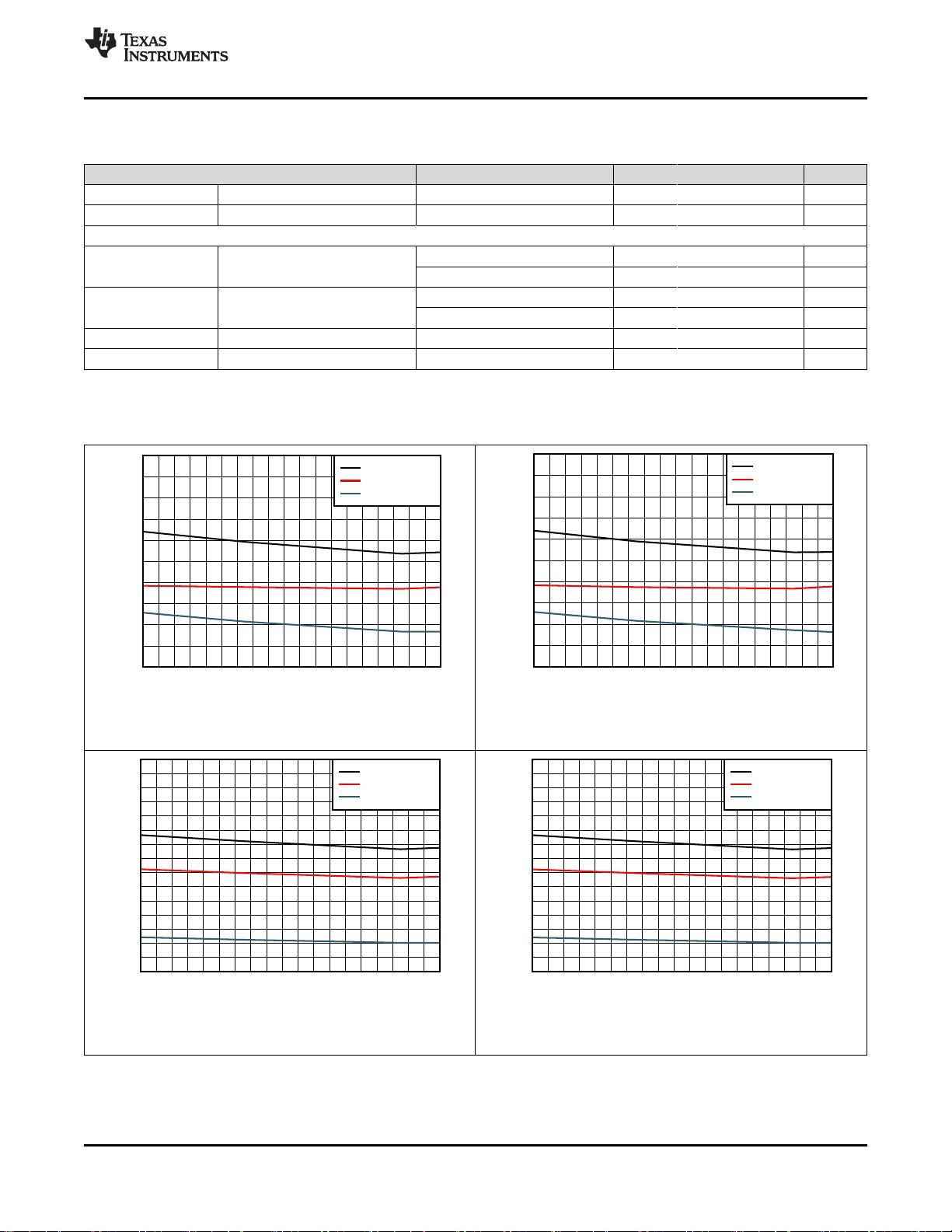
• 磁性灵敏度选项 (B
OP
,B
RP
):
– DRV5021A1-Q1:2.9mT、1.8mT
– DRV5021A2-Q1:9.2mT、7.0mT
– DRV5021A3-Q1:17.9mT、14.1mT
• 30kHz 高速感应带宽
• 漏极开路输出电流高达 20mA
• 经过优化的低电压架构
• 具有集成迟滞特性,可增强抗噪能力
• 标准行业封装:
– 表面贴装 SOT-23
2 应应用用
• 汽车变速器、车身外壳
• 限位开关
• 一般接近感应
• 刷式直流电机反馈
• 门开关检测
• 阀定位
• 脉冲计数
3 说说明明
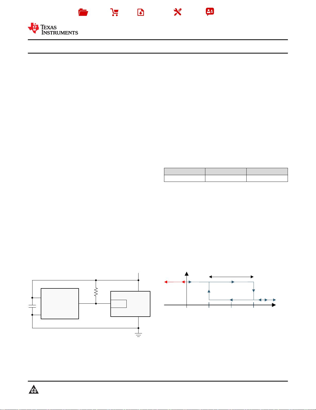
DRV5021-Q1 是一款低电压数字开关霍尔效应传感
器,适用于高速汽车 应用。该器件由 2.5V 至 5.5V 的
电源供电,可以检测磁通量密度并根据预定义的磁性阈
值提供数字输出。
该器件会检测垂直于封装面的磁场。当施加的磁通量密
度超过磁运行点 B
OP
阈值时,器件的漏极开路输出将
驱动低电压。当磁通量密度降至磁释放点 (B
RP
) 阈值
时,输出会变为高阻抗。B
OP
和 B
RP
的分离所产生的
滞后有助于防止输入噪声引起的输出误差。这种配置使
得系统设计能够更加稳健地抵抗噪声干扰。
该器件可在 –40°C 至 +150°C 的宽环境温度范围内保
持稳定的优异性能。
器器件件信信息息
(1)
器器件件型型号号 封封装装 封封装装尺尺寸寸((标标称称值值))
DRV5021-Q1 SOT-23 (3) 2.90mm x 1.30mm
(1) 如需了解所有可用封装,请参阅数据表末尾的封装选项附录。
典典型型应应用用电电路路原原理理图图 磁磁响响应应


剩余25页未读,继续阅读
资源评论

 不觉明了2023-05-15#完美解决问题 #运行顺畅 #内容详尽 #全网独家 #注释完整

2301_77771913
- 粉丝: 1
- 资源: 30


最新资源
- 基于原生微信小程序实现的课堂考勤系统的设计与实现
- 商道融绿、润灵环球ESG评级数据(2015-2023年).xlsx
- 商道融绿、润灵环球ESG评级数据(2015-2023年).dta
- 基于 GDAL 与 PROJ4 的遥感图像处理软件,使用 Qt 构建课程设计
- 图形化界面采用Easyx编写,实现对哈夫曼树的显示操作
- 使用后端开发框架Spring Boot构建应用程序.pdf
- 基于Boson的计算机网络实验:RIP和IGRP的配置
- 在线教育系统 JAVA+Vue+SpringBoot+MySQL
- 健身房管理系统 JAVA+Vue+SpringBoot+MySQL
- 卓越导师双选系统 JAVA+Vue+SpringBoot+MySQL
资源上传下载、课程学习等过程中有任何疑问或建议,欢迎提出宝贵意见哦~我们会及时处理!
点击此处反馈


