
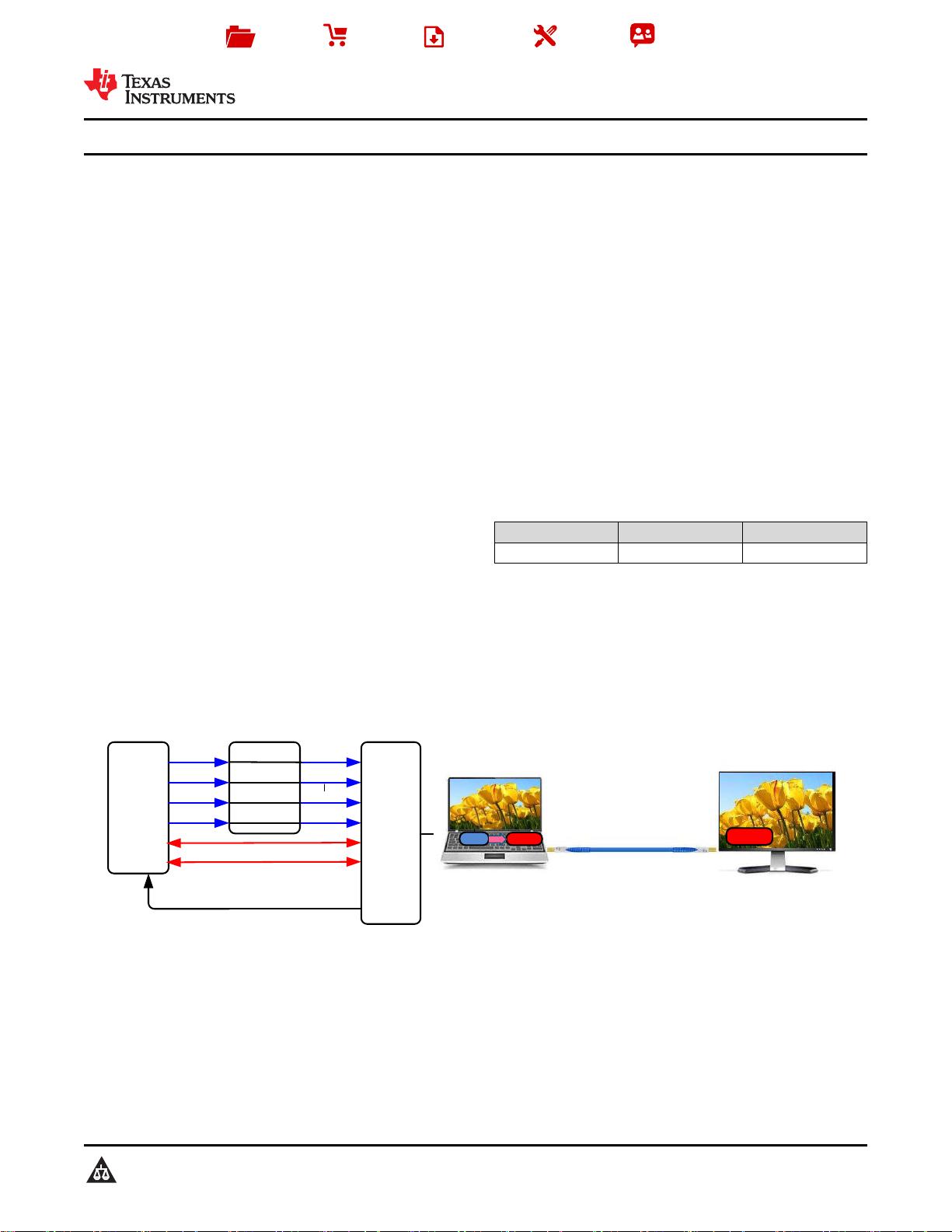
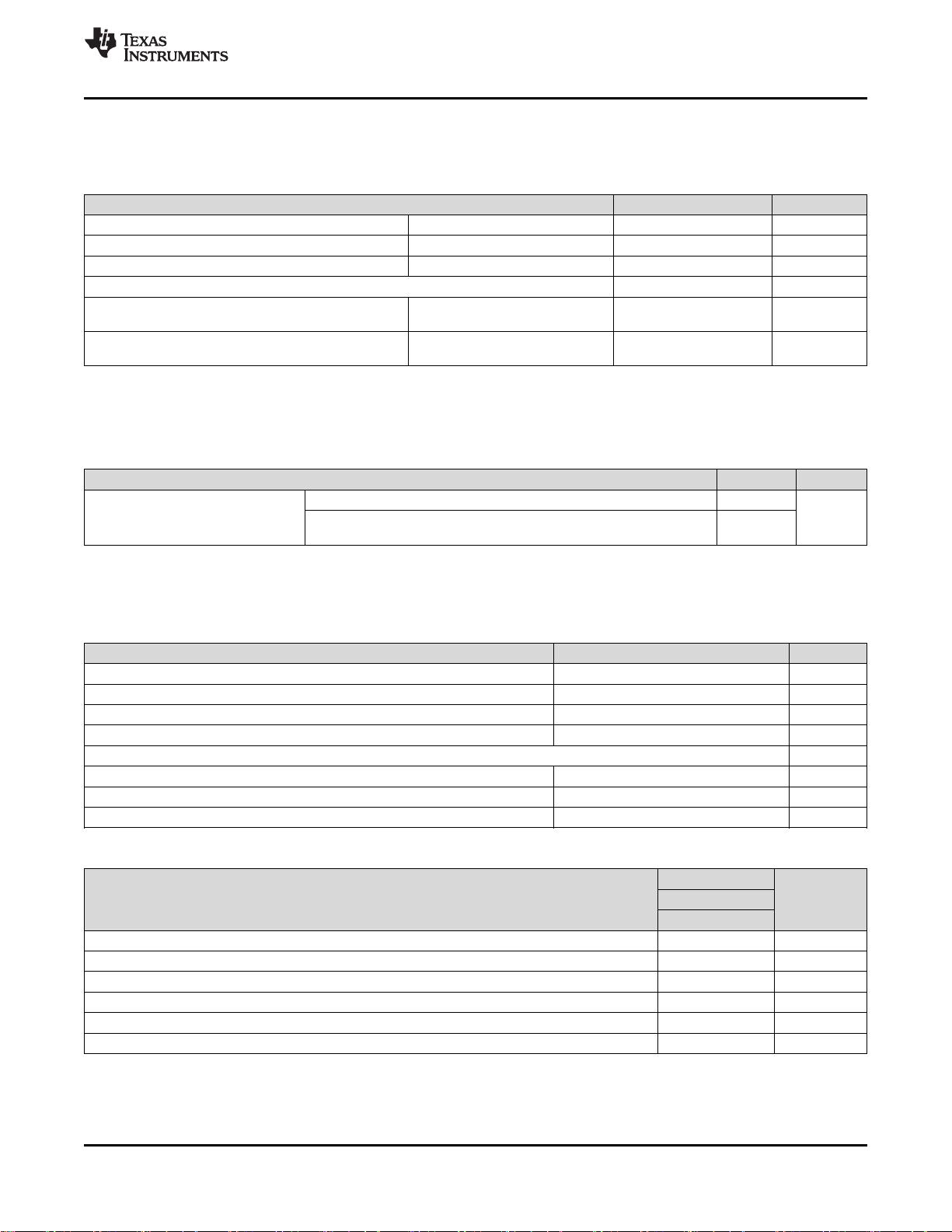
GPU
DP141
OUTP0
DisplayPort Connector
HPD
ML0
x
GPU
x
DP141
x
DP141
DP0
AUXp
DP1
DP2
DP3
HPD
AUXn
OUTP1
OUTP2
OUTP3
ML1
ML2
ML3
AUXp
AUXn
Product
Folder
Sample &
Buy
Technical
Documents
Tools &
Software
Support &
Community
An IMPORTANT NOTICE at the end of this data sheet addresses availability, warranty, changes, use in safety-critical applications,
intellectual property matters and other important disclaimers. PRODUCTION DATA.
English Data Sheet: SLLSES6
SN65DP141
ZHCSEQ7 –FEBRUARY 2016
SN65DP141 DisplayPort 线线性性转转接接驱驱动动器器
1
1 特特性性
1
• 支持 VESA DisplayPort 1.3 和 eDP 1.4
• 四通道线性转接驱动器,最高支持 12Gbps 的数据
速率,包括 DisplayPort RBR、HBR、HBR2 和
HBR3
• 与协议无关
• 对 DP 链路协商透明
• 与在链路上的位置无关,适用于源设备、接收设备
和电缆 应用
• 6GHz 时的 15dB 模拟均衡
• 输出线性动态范围:1200mV
• 带宽:> 20GHz
• 6GHz 时的回波损耗优于 16dB
• 2.5V 或 3.3V ±5% 单电源选项
• 低功耗,2.5V V
CC
时每通道 80mW
• 通用输入输出接口 (GPIO) 或者 I
2
C 控制
2 应应用用
• 平板电脑
• 笔记本电脑
• 台式机
• 扩展坞
3 说说明明
SN65DP141 是一款与协议无关的异步、低延迟、四通
道线性均衡器,该器件经过优化适用于高达 12Gbps
的数据速率并且可对电路板走线和电缆所产生的损耗进
行补偿。
该器件对 DisplayPort (DP) 链路协商透明,这使得 DP
源设备和接收设备能够执行有效的链路协商,克服了传
统“aux snooping”转接驱动器的缺点。此外,该器件与
位置无关。它可置于源设备、电缆或接收设备内,从而
为总体链路预算有效提供“负损耗”分量。SN65DP141
内的线性均衡在与接收器搭配使用时还可提高链路裕
度,从而实现判决反馈均衡 (DFE)。
SN65DP141 支持采用 I
2
C 和 GPIO 配置对均衡、增
益、动态范围进行独立通道控制。
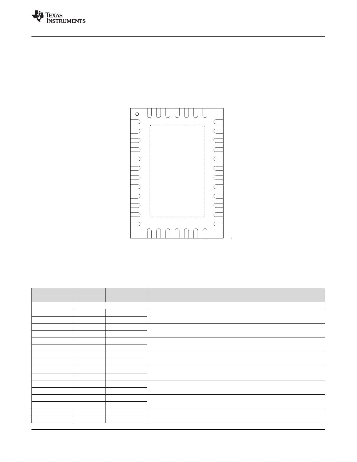
器器件件信信息息
(1)
器器件件型型号号 封封装装 封封装装尺尺寸寸((标标称称值值))
SN65DP141 WQFN (38) 7.00mm x 5.00mm
(1) 要了解所有可用封装,请参见数据表末尾的可订购产品附录。
空白
空白
简简化化电电路路原原理理图图
剩余34页未读,继续阅读
资源评论


不觉明了
- 粉丝: 6209
- 资源: 5760


最新资源
- 几何物体检测44-YOLO(v5至v11)、COCO、CreateML、Paligemma、TFRecord、VOC数据集合集.rar
- 几何物体检测43-YOLO(v5至v9)、COCO、CreateML、Paligemma、TFRecord、VOC数据集合集.rar
- 基于cruise的燃料电池功率跟随仿真,按照丰田氢能源车型搭建,在wltc工况下跟随效果好,最高车速175,最大爬坡30,百公里9s均已实现 1.模型通过cruise simulink联合仿真,策略
- C#源码 上位机 联合Visionpro 通用框架开发源码,已应用于多个项目,整套设备程序,可以根据需求编出来,具体Vpp功能自己编 程序包含功能 1.自动设置界面窗体个数及分布 2.照方式以命令触
- 程序名称:悬架设计计算程序 开发平台:基于matlab平台 计算内容:悬架偏频刚度挠度;螺旋弹簧,多片簧,少片簧,稳定杆,减震器的匹配计算;悬架垂向纵向侧向力学、纵倾、侧倾校核等;独立悬架杠杆比,等效
- 华为OD+真题及解析+智能驾驶
- jQuery信息提示插件
- 基于stm32的通信系统,sim800c与服务器通信,无线通信监测,远程定位,服务器通信系统,gps,sim800c,心率,温度,stm32 由STM32F103ZET6单片机核心板电路、DS18B2
- 充电器检测9-YOLO(v5至v11)、COCO、Create充电器检测9L、Paligemma、TFRecord、VOC数据集合集.rar
- 华为OD+考试真题+实现过程
资源上传下载、课程学习等过程中有任何疑问或建议,欢迎提出宝贵意见哦~我们会及时处理!
点击此处反馈


