没有合适的资源?快使用搜索试试~ 我知道了~
TI-UC3872.pdf
需积分: 10 0 下载量 49 浏览量
2022-11-19
23:38:41
上传
评论 5
收藏 381KB PDF 举报
温馨提示
试读
11页
TI-UC3872.pdf
资源推荐
资源详情
资源评论
UC1872
UC2872
UC3872
07/99
FEATURES
•
Controls Different Types of Lamps:
Cold Cathode Fluorescent, Neon, and
Gas Discharge
•
Zero Voltage Switching (ZVS) of
Push-Pull Drivers
•
Accurate Control of Lamp Current
•
Variable Lamp Intensity Control
•
1µA Disable Current
•
4.5V to 24V Operation
•
Open Lamp Detection Circuitry
DESCRIPTION
The UC3872 is a resonant lamp ballast controller optimized for driving
cold cathode fluorescent, neon, and other gas discharge lamps. The res
-
onant power stage develops a sinusoidal lamp drive voltage, and mini
-
mizes switching loss and EMI generation. Lamp intensity adjustment is
accomplished with a buck regulator, which is synchronized to the external
power stage’s resonant frequency. Suitable for automotive and battery
powered applications, the UC3872 draws only 1µA when disabled.
Soft start and open lamp detect circuitry have been incorporated to mini
-
mize component stresses. Open lamp detection is enabled at the comple
-
tion of a soft start cycle. The chip is optimized for smooth duty cycle
control to 100%.
Other features include a precision 1.2% reference, undervoltage lockout,
and accurate minimum and maximum frequency control.
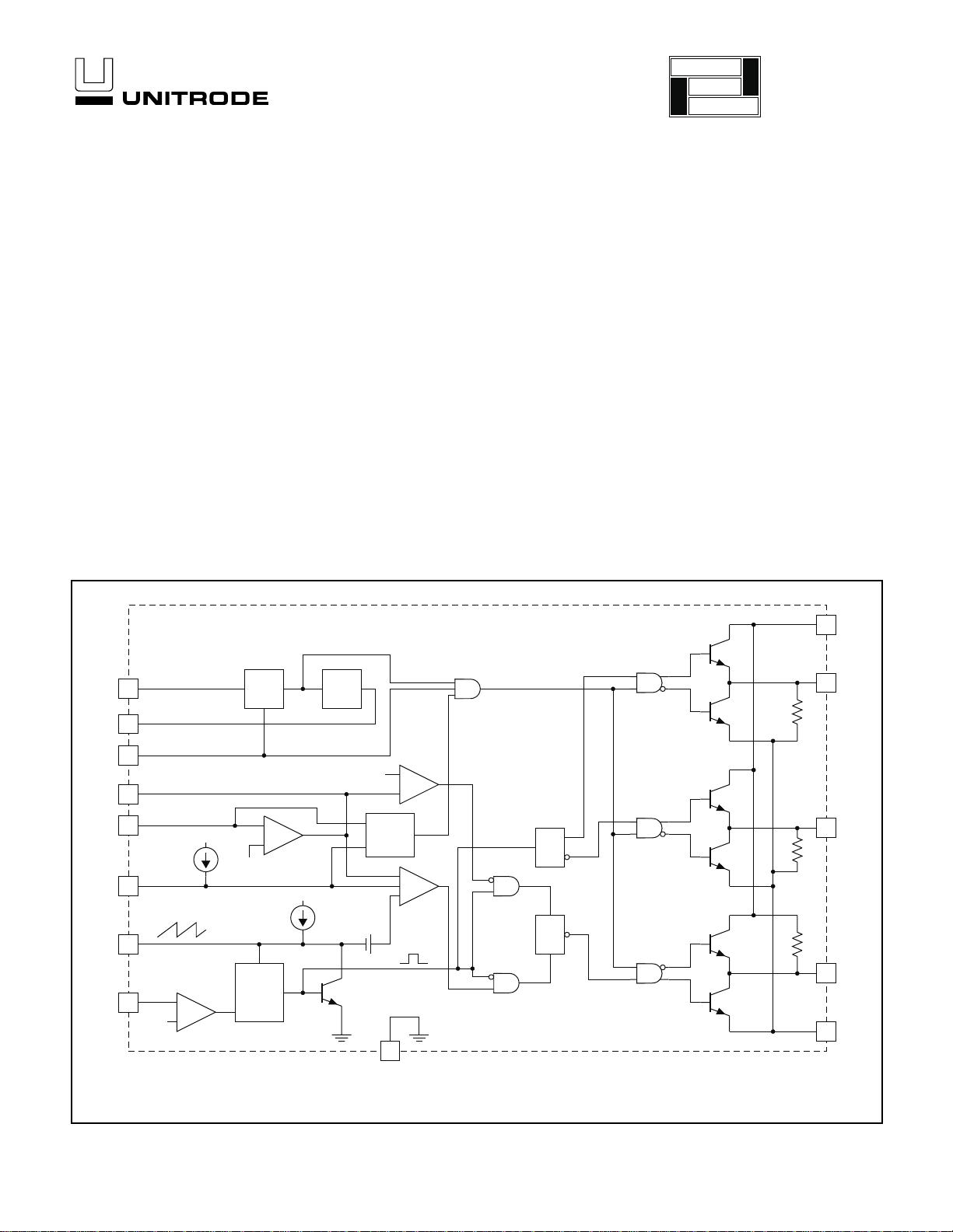
Resonant Lamp Ballast Controller
4
6
5
3
2
12
13
1
14
7
8
+
–
0.5V
SYNC
OUT
SENSE
OSCILLATOR
GND
+
–
–
+
OPEN
LAMP
DETECT
+
–
+
–
UVLO
3.0V
REF
10
9
11
R
S
T
TOGGLE
50k
50k
50k
PUSH PULL
OUTPUTS
N-CHANNEL
VC
AOUT
BOUT
COUT
PGND
0.1V
PWM
1
0.2V
200µA
ZERO DETECT
ZD
CT
SS
INV
COMP
ENBL
REF
VCC
1.5V
20µA
(HIGH=ENABLE)
BUCK DRIVE
P-CHANNEL
EA
BLOCK DIAGRAM
UDG-99112
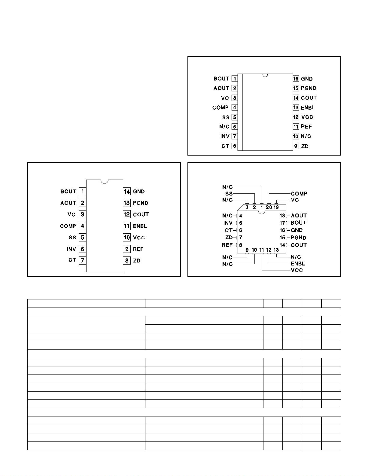
Note: Pin numbers shown are for DIP package.
application
INFO
available
2
UC1872
UC2872
UC3872
ELECTRICAL CHARACTERISTICS:
Unless otherwise stated, these parameters apply for TJ = −55°C to +125°C for the
UC1872, –40°C to +85°C for the UC2872, −0°C to +70°C for the UC3872; VCC= 5V, VC = 15V, V
ENBL
= 5V, CT = 1nF, ZD = 1V.
PARAMETER TEST CONDITIONS MIN TYP MAX UNITS
Reference Section
Output Voltage T
J = 25°C 2.963 3.000 3.037 V
Over Temperature 2.940 3.000 3.060 V
Line Regulation VCC = 4.75V to 18V 10 mV
Load Regulation I
O
= 0 to −5mA 10 mV
Oscillator Section
Free Running Frequency T
J
= 25°C 576878kHz
Maximum Synchronization Frequency T
J
= 25°C 160 200 240 kHz
Charge Current V
CT
= 1.5V 180 200 220 µA
Voltage Stability 2%
Temperature Stability 48%
Zero Detect Threshold 0.46 0.5 0.56 V
Error Amp Section
Input Voltage V
O
= 2V 1.445 1.475 1.505 V
Input Bias Current −0.4 −2 µA
Open Loop Gain V
O
= 0.5 to 3V 65 90 dB
Output High V
INV
= 1.3V 3.1 3.5 3.9 V
ABSOLUTE MAXIMUM RATINGS
Analog Inputs . . . . . . . . . . . . . . . . . . . . . . . . . . . . . −0.3 to +10V
VCC, VC Voltage. . . . . . . . . . . . . . . . . . . . . . . . . . . . . . . . +24V
ZD Input Current
High Impedance Source . . . . . . . . . . . . . . . . . . . . . . +10mA
ZD Input Voltage
Low Impedance Source . . . . . . . . . . . . . . . . . . . . . . . . +24V
Power Dissipation at T
A = 25°C . . . . . . . . . . . . . . . . . . . . . . 1W
Storage Temperature . . . . . . . . . . . . . . . . . . . −65°C to +150°C
Lead Temperature. . . . . . . . . . . . . . . . . . . . . . . . . . . . . . 300°C
Note 1: Currents are positive into, negative out of the specified
terminal.
Note 2: Consult Packaging Section of Databook for thermal limi
-
tations and considerations of package.
DIL-14 (TOP VIEW)
N Package
PLCC-20 (Top View)
Q Package
CONNECTION DIAGRAMS
SOIC-16, SSOP-16 (TOP VIEW)
DW, M Package
3
UC1872
UC2872
UC3872
ELECTRICAL CHARACTERISTICS:
Unless otherwise stated, these parameters apply for TJ = −55°C to +125°C for the
UC1872, –40°C to +85°C for the UC2872, −0°C to +70°C for the UC3872; VCC= 5V, VC = 15V, V
ENBL
= 5V, CT = 1nF, ZD = 1V.
PARAMETER TEST CONDITIONS MIN TYP MAX UNITS
Error Amp Section (cont.)
Output Low V
INV
= 1.7V 0.1 0.2 V
Output Source Current V
INV
= 1.3V, V
O
= 2V –350 –500 µA
Output Sink Current V
INV
= 1.7V, V
O
= 2V 10 20 mA
Common Mode Range 0V
IN
-1V V
Unity Gain Bandwidth T
J
= 25°C (Note 4) 1 MHz
Open Lamp Detect Section
Soft Start Threshold V
INV
= 0V 2.9 3.4 3.8 V
Open Lamp Detect Threshold V
SS
= 4.2V 0.6 1.0 1.4 V
Soft Start Current V
SS
= 2V 10 20 40 µA
Output Section
Output Low Level I
OUT
= 0, Outputs A and B 0.05 0.2 V
I
OUT
= 10mA 0.1 0.4 V
I
OUT
= 100mA 1.5 2.2 V
Output High Level I
OUT
= 0, Output C 13.9 14.9 V
I
OUT
= −10mA 13.5 14.3 V
I
OUT
= −100mA 12.5 13.5 V
Rise Time T
J
= 25°C, Cl = 1nF (Note 4) 30 80 ns
Fall Time T
J
= 25°C, Cl = 1nF (Note 4) 30 80 ns
Output Dynamics
Out A and B Duty Cycle 48 49.9 50 %
Out C Max Duty Cycle V
INV
= 1V 100 %
Out C Min Duty Cycle V
INV
= 2V 0 %
Under Voltage Lockout Section
Startup Threshold Voltage 3.7 4.2 4.5 V
Hysteresis 120 200 280 mV
Enable Section
Input High Threshold 2V
Input Low Threshold 0.8 V
Input Current V
ENBL
= 5V 150 400 µA
Supply Current Section
VCC Supply Current VCC = 24V 6 14 mA
VC Supply Current VC = 24V 5 12 mA
ICC Disabled VCC = 24V, V
ENBL = 0V 1 10 µA
Note 3: Unless otherwise specified, all voltages are with respect to ground. Currents are positive into, and negative out of the
specified terminal.
Note 4: Guaranteed by design. Not 100% tested in production.
剩余10页未读,继续阅读
资源评论
不觉明了
- 粉丝: 3164
- 资源: 5419
上传资源 快速赚钱
- 我的内容管理 展开
- 我的资源 快来上传第一个资源
- 我的收益 登录查看自己的收益
- 我的积分 登录查看自己的积分
- 我的C币 登录后查看C币余额
- 我的收藏
- 我的下载
- 下载帮助
安全验证
文档复制为VIP权益,开通VIP直接复制
信息提交成功